
Figures & data
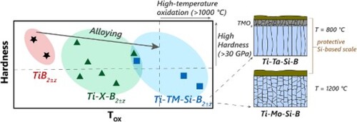
Table 1. Chemical composition, crystallographic parameters (c/a ratio), and mechanical properties (H and E) for all grown Ti-(TM)-Si-B2 ± z coating materials.
Figure 1. X-ray diffractograms of (a) TiB2.57, (b) Ti-Si-B2 ± z, (c) Ti-Ta-Si-B2 ± z, and (d) Ti-Mo-Si-B2 ± z alloyed coatings with their stoichiometries indicated.
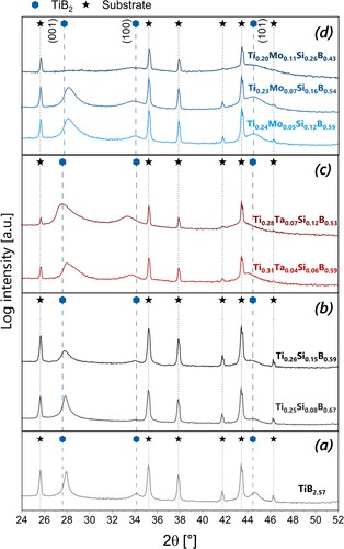
Figure 2. Thermogravimetric (TG) curves of mass change during dynamic oxidation of (a) Ti-Si-B2 ± z, (b) Ti-Ta-Si-B2 ± z, and (c) Ti-Mo-Si-B2 ± z coatings in synthetic air under heating rate of 10°C/min. The TG curve for the binary coating TiB2.57 is indicated by a dashed line in (a), (b) and (c).
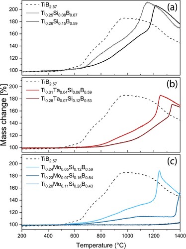
Figure 3. TEM analysis of Ti0.28Ta0.07Si0.12B0.53 coating oxidized in ambient air at 800°C for 1 h. (a) BF image of the whole coating with the substrate at the bottom and oxide scale on top. (b) magnified area of the oxide scale with coating interface. (c) SAED image for the area indicated in (a). (d) STEM image and corresponding EELS maps for the area illustrated in (b).
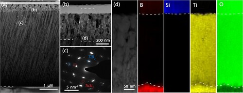
Figure 4. TEM analysis of Ti0.23Mo0.07Si0.16B0.54 coating oxidized in ambient air at 1200°C for 1 h. (a) BF image of the whole coating with the substrate at the bottom and oxide scale on top. (b) magnified area for oxide scale with coating interface. (c1) and (c2) SAED patterns for areas indicated in (a). (d) elemental EELS maps for the area illustrated in (b).
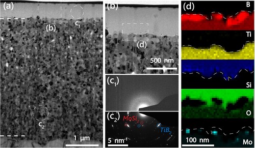
Figure 5. As-deposited hardness of diverse alloyed TiB2 ± z coatings in relation to their oxidation temperature Tox. The obtained scale thickness (at Tox) for each coating is indicated in relation to the reported oxidation time. The as-deposited coating thicknesses are: 2 µm for Ti0.26Si0.15B0.59, 4.9 µm for Ti0.28Ta0.07Si0.12B0.53, 3.5 µm for Ti0.23Mo0.07Si0.16B0.54, 4.9 µm for Ti0.20Mo0.11Si0.16B0.54, 400 nm for TiB1.43 [Citation16], 980 nm for Ti0.9Al0.1B1.3 [Citation26], 1.3 µm for (Ti0.35Al0.65)B2 [Citation25], ∼1.5 µm for (Ti0.68Al0.32)B1.35 [Citation18],and ∼1.4 µm for Ti0.13Si0.41B0.46 [Citation27].
![Figure 5. As-deposited hardness of diverse alloyed TiB2 ± z coatings in relation to their oxidation temperature Tox. The obtained scale thickness (at Tox) for each coating is indicated in relation to the reported oxidation time. The as-deposited coating thicknesses are: 2 µm for Ti0.26Si0.15B0.59, 4.9 µm for Ti0.28Ta0.07Si0.12B0.53, 3.5 µm for Ti0.23Mo0.07Si0.16B0.54, 4.9 µm for Ti0.20Mo0.11Si0.16B0.54, 400 nm for TiB1.43 [Citation16], 980 nm for Ti0.9Al0.1B1.3 [Citation26], 1.3 µm for (Ti0.35Al0.65)B2 [Citation25], ∼1.5 µm for (Ti0.68Al0.32)B1.35 [Citation18],and ∼1.4 µm for Ti0.13Si0.41B0.46 [Citation27].](/cms/asset/93dd14e3-86e5-43a2-bae0-65e9cf2b6668/tmrl_a_2225554_f0005_oc.jpg)