Figures & data
Table 1. Relative density and average grain size of specimens after microwave and conventional sintering
Figure 1. FE-SEM microstructure of samples: NK00 (a) MW 1200°C-10 min, (b) MW 1300°C-10 min, (c) CS 1400°C-1 h, and NK10 (d) MW 1200°C-10 min, (e) MW 1300°C-10 min and (f) CS 1400°C-1 h
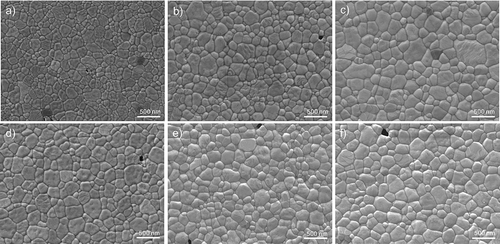
Figure 2. Vickers hardness values of NK samples
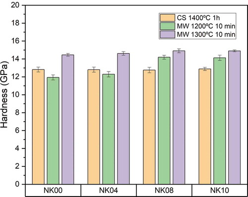
Figure 3. Fracture toughness values of NK samples
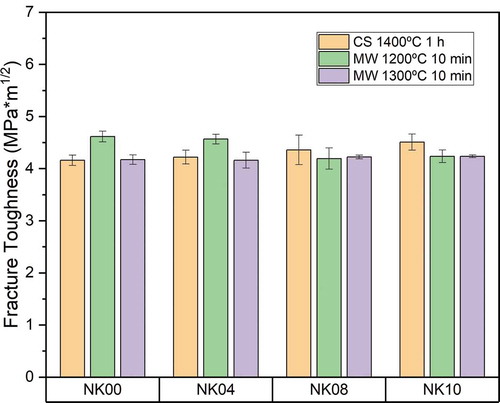
Figure 4. Raman shift of samples sintered in CS at 1400°C and MW at 1300°C after 40 h of LTD exposure
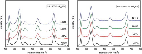
Table 2. CIELAB coordinates for doped NK samples
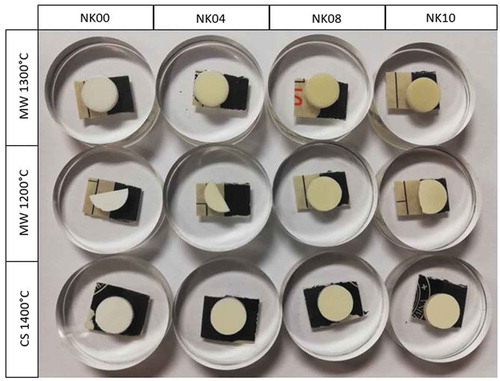
Figure 5. Image of zirconia color samples doped with different quantities of Fe2O3 sintered by MW and CS