Figures & data
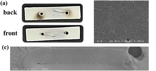
Figure 1. Flash onset conditions for flash sintering in air or in vacuum
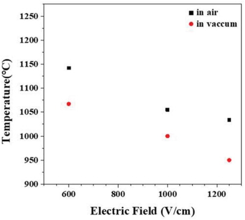
Figure 2. Change of the incubation time for the occurrence of flash with a change of temperature and electric field
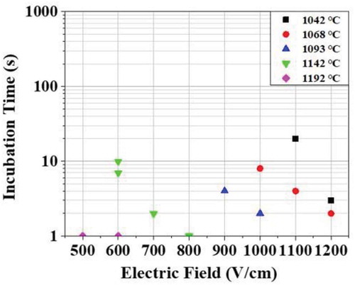
Figure 3. Electric current density and temperature rise of the sample during flashing under the various electric field
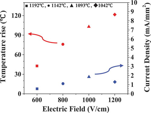
Figure 4. Density of samples prepared by flash or normal sintering
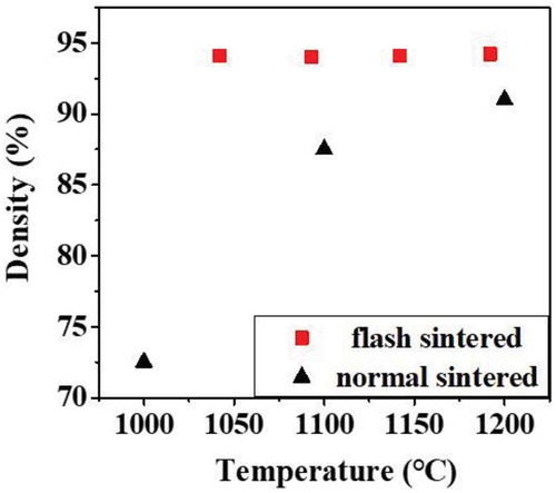
Figure 5. X-ray diffractometry pattern of the samples produced by flash sintering in the condition of (a) 1192 °C 0 V/cm, (b) 1192 °C 600 V/cm, (c) 1142 °C 800 V/cm, (d) 1093 °C 1000 V/cm, (e) 1042 °C 1200 V/cm, and of (f) hydroxyapatite powders, and (g) JCPDS file (9-432) of hydroxyapatite
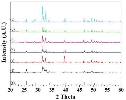
Figure 6. SEM image of the cross-sectional microstructure of the samples prepared by (a) flash sintering at 1051 °C 1000 V/cm for 10 seconds, and (b) normal sintering at 1192°C for one hour
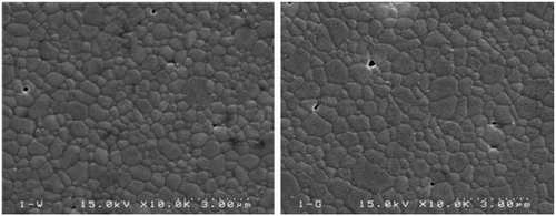
Figure 7. Transmission electron microscope image of hydroxyapatite sample prepared by flash sintering
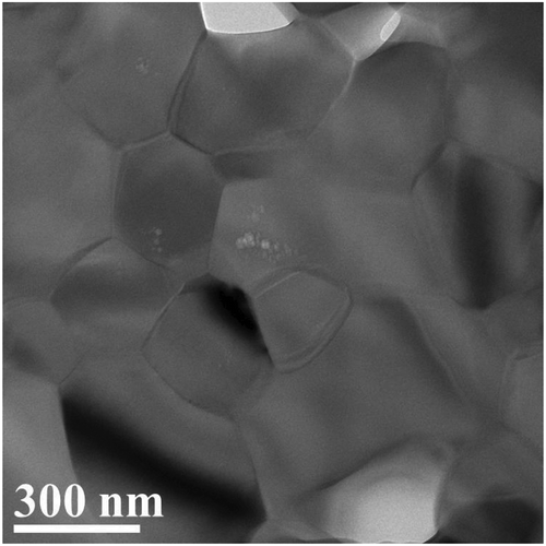
Figure 8. A sample with partial melting during flash sintering, (a) Front and back surface images of the flash sintered sample under the condition of 1000 V/cm, One can see band-like melt trace between the two electrode holes. (b) A cross-sectional microstructure under the melt trace (c) low magnification(x50) image of the melt trace. One can see splash