Figures & data
Table 1. Deposition methods, substrates, and corresponding substrate temperatures.
Figure 1. Schematic of the CO2 laser-assisted RF sputtering system.
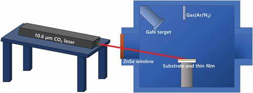
Figure 2. X-ray diffraction patterns of the RF-sputtered GaN thin films deposited on sapphire substrates at the temperature of 200°C, RF power of 200 W, and working pressure of 15 mTorr, with different Ar partial pressure conditions (a) – (d) and without thin-film fabrication process (e).
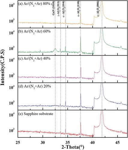
Figure 3. X-ray diffraction patterns of the RF-sputtered GaN thin films deposited on sapphire substrates at the temperature of 200°C, working pressure of 15 mTorr, with different RF power conditions (a) – (c) and without thin-film fabrication process (d).
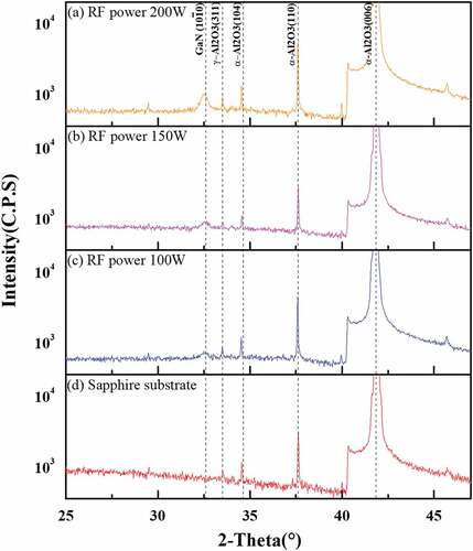
Figure 4. X-ray diffraction patterns of the CO2-laser-assisted RF-sputtered GaN thin films deposited on a sapphire substrate by varying the energy density of the CO2 laser. Process conditions: Ar partial pressure 60%, RF power 200 W, working pressure 15 mTorr, and substrate temperature 200°C (a) – (e). GaN thin film without CO2 laser assistance (f) and without thin-film fabrication process (g).
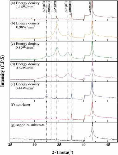
Table 2. Surface energy of the (0001), (1120), (1011), and (1010) planes of GaN wurtzite.
Figure 5. X-ray diffraction pattern peak ratios in (0002), (1010) and (1011) orientations of CO2 laser-assisted RF sputtered GaN thin films fabricated at different laser energy densities.
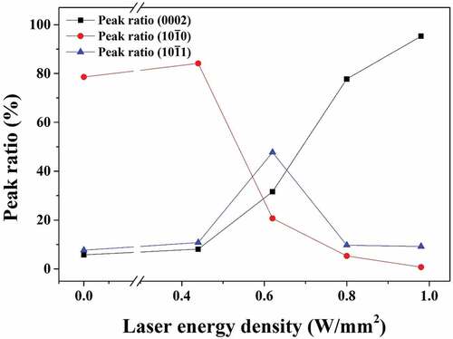
Figure 6. Transmittance and Tauc plot of the CO2 laser-assisted RF-sputtered GaN thin films fabricated at different laser energy densities. The insert shows the simulated bandgaps of the GaN thin films from the transmittance values.
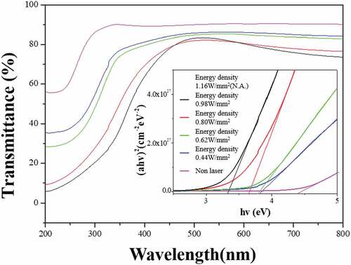
Figure 7. Bandgaps of the CO2 laser-assisted RF-sputtered GaN thin films fabricated at different laser energy densities.
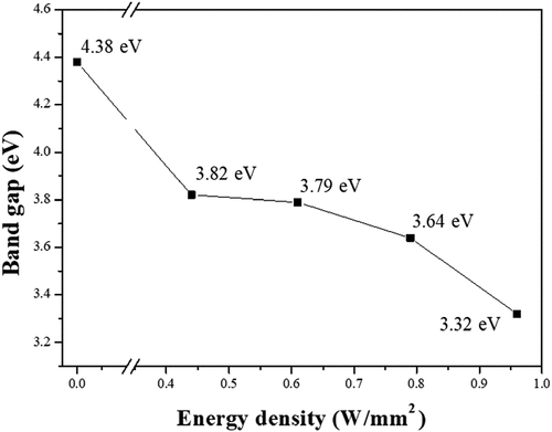
Figure 8. Scanning electron microscopy (SEM) images of the CO2 laser-assisted RF-sputtered GaN thin films fabricated at different laser energy densities.
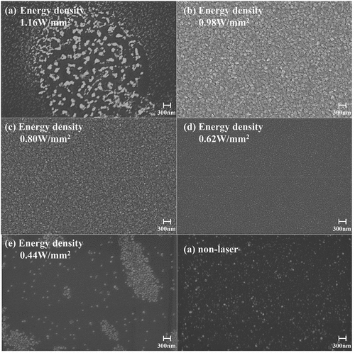
Figure 9. Scanning electron microscopy (SEM) surface images (a)-(e), cross-sectional images (f) of CO2 laser-assisted RF sputtered GaN thin films fabricated at a laser energy density of 0.98 W/mm2.
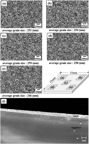
Figure 10. High-resolution scanning electron microscopy (SEM) images of the CO2 laser-assisted RF sputtered GaN thin films fabricated at different laser energy densities.
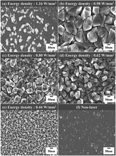
Figure 11. Photoluminescence (PL) wavelength of the CO2 laser-assisted RF-sputtered GaN thin films fabricated at different laser energy densities.
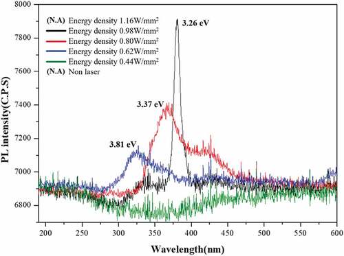
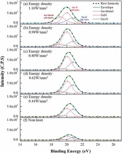
Figure 12. X-ray photoelectron spectroscopy (XPS) spectra of the Ga 3d core level of the CO2 laser-assisted RF-sputtered GaN thin films deposited on a sapphire substrate by varying the energy density of the CO2 laser. Process conditions: Ar partial pressure 60%, RF power 200 W, working pressure 15 mTorr, substrate temperature 200°C.