
Figures & data
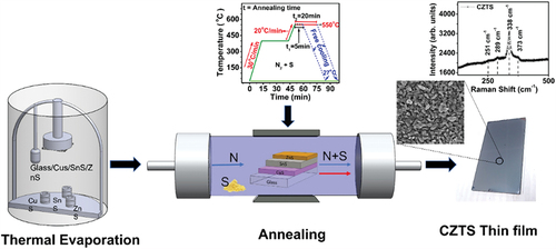
Figure 1. Temperature vs. time profile used in the sulfurization-crystallization process.
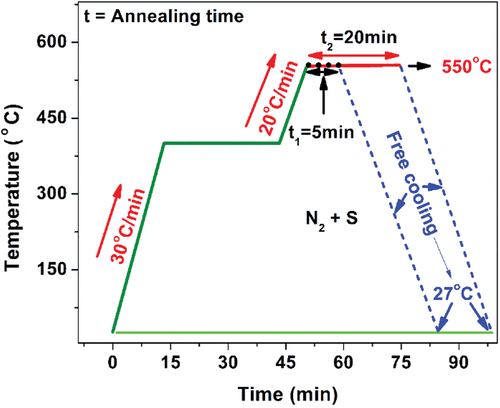
Figure 2. XRD patterns of CZTS thin films. a) as deposited, and sulfurised in Ar + S ambient at 550°C for b) 5 min, and c) 20 min. Standard powder diffraction patterns of Cu2ZnSnS4 (PDF # 26–0575) are shown in d).
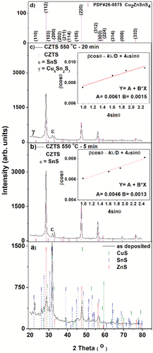
Table 1. Lattice parameter, crystal size measured by Scherrer and Williamson–Hall method, deformation, and degree of preferential orientation of the sulfide films annealed in Ar + S at 550°C for 5 and 20 min. In all cases, a fixed amount of sulfur (5 mg) was used.
Figure 3. Raman spectra of CZTS films. a) as-deposited, and sulfurised in Ar + S ambient at 550°C for b) 5 min and c) 20 min.
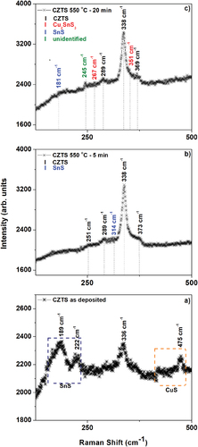
Table 2. Elemental composition (at %) of CZTS films annealed at 550℃ for different time durations.
Figure 4. SEM images of the sulfurised CZTS thin films in Ar + S ambient at 550°C for a) 5 min and b) 20 min. c) shows the cross-section image of the film annealed for 5 min.
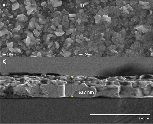
Figure 5. A) Surface and c) cross-sectional EDXS analysis of a CZTS film heat-treated at 550℃ for 5 minutes, the rectangular region marked with yellow boundaries in (a) and the vertical line in (c) indicates the selected region of EDXS analysis. b) and d) are the EDXS spectra.
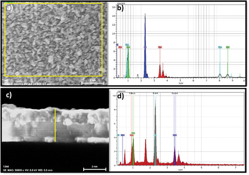
Figure 6. AFM images of the CZTS films annealed for a) 5 min and b) 20 min.
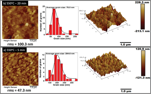
Figure 7. A) Graph of the optical absorption coefficient of CZTS films. The inset shows the transmittance (T%) of the films. b) Plot of for the band gap estimation. The inset shows the Urbach plot (
).The annealing times are shown in each plot.
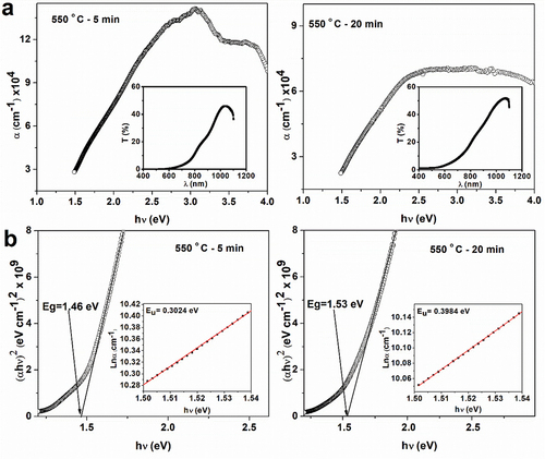
Figure 8. Photocurrent response of CZTS thin films annealed at 550°C for time durations a) 5 min. and b) 20 min. The best fit to EquationEq. (6)(6)
(6) is represented with the red line, the photosensitivity
and the decay time (
are indicated in the figure.
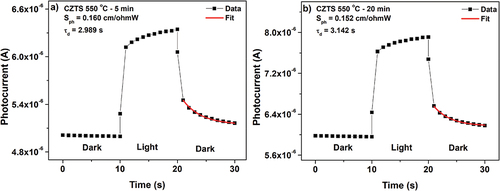
Table 3. Dark and light conductivity, and photosensitivity of the CZTS thin films annealed at 550°C for time durations 5 and 20 min.