Figures & data
Figure 1. Block diagram of digital filtering process.
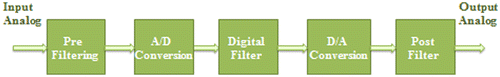
Figure 2. Block diagram of FIR filter.
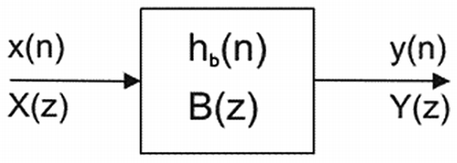
Figure 3. Basic structure of FIR filter.
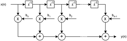
Figure 4. Design stages of digital filters.
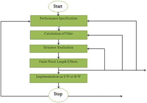
Table 1. Filter specifications
Figure 5. FIR BPF using Hanning window.
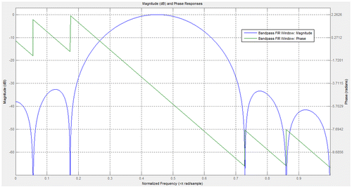
Figure 6. FIR BPF using Hamming window.
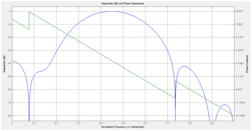
Figure 7. FIR BPF using Blackman window.
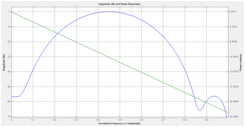
Figure 8. FIR BPF using Kaiser window.
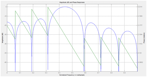
Table 2. Comparison of 15th-order fir BPF using different window functions
Figure 9. Frequency response of FIR band pass filter with no quantization.
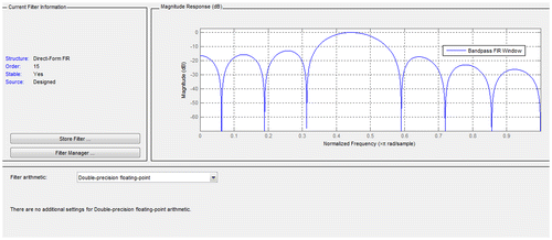
Figure 10. BPF 1 (Quantization [16, 15] of FIR band pass filter).
![Figure 10. BPF 1 (Quantization [16, 15] of FIR band pass filter).](/cms/asset/9bd4ee19-fbe9-4028-a9ce-192c19c08432/oaen_a_1323373_f0010_oc.gif)
Figure 11. BPF 2 (Quantization [8, 7] of FIR band pass filter).
![Figure 11. BPF 2 (Quantization [8, 7] of FIR band pass filter).](/cms/asset/1d42277d-94ef-4794-8085-5c794b300676/oaen_a_1323373_f0011_oc.gif)
Figure 12. BPF 3 (Quantization [6, 5] of FIR band pass filter).
![Figure 12. BPF 3 (Quantization [6, 5] of FIR band pass filter).](/cms/asset/5b5185e0-d4cd-45d2-8dec-02ca7a16cb97/oaen_a_1323373_f0012_oc.gif)
Figure 13. BPF 4 (Quantization [3, 2] of FIR band pass filter).
![Figure 13. BPF 4 (Quantization [3, 2] of FIR band pass filter).](/cms/asset/5ade4964-7378-41ca-ac08-502c205eff54/oaen_a_1323373_f0013_oc.gif)
Table 3. Performance characteristics of filters
Figure 14. Simulink model of FIR band pass filter.
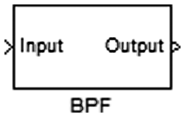
Figure 15. Structure & coefficients of 15-order BPF.
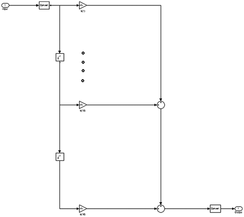
Figure 16. ASIC design flow.
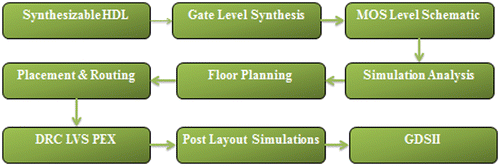
Figure 17. Input and output waveform.
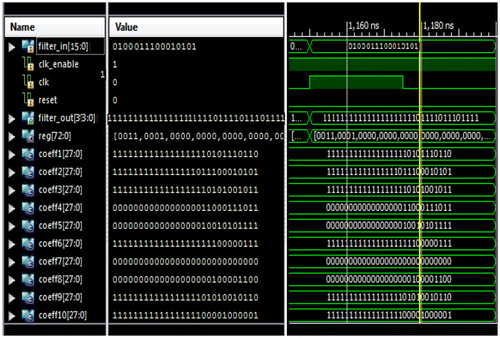
Figure 18. Top module of 15-order band pass filter.
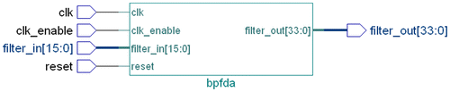
Figure 19. Complete RTL schematic of BPF.
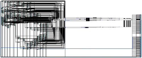
Figure 20. Complete gate level schematic of BPF.
Figure 21. Pyxis schematic of 12th Sheet.
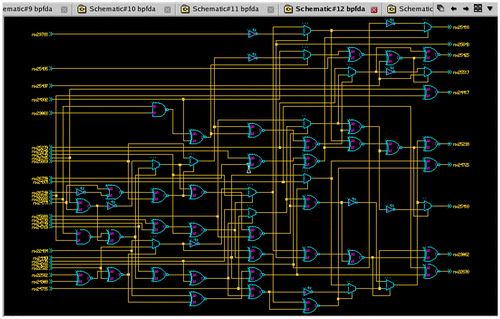
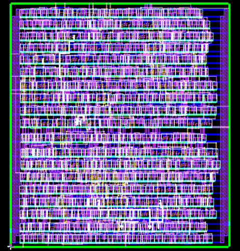
Figure 22. Layout of 15-order band pass filter.