
Figures & data
Figure 1. Typical block diagram of RF energy harvesting circuit.
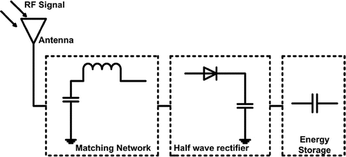
Figure 2. (a) Circuit diagram of the proposed dual-band rectifier circuit and (b) optimized dual-band rectifier circuit.
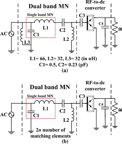
Figure 3. Conversion of a single-band matching network to dual-band matching network using frequency transformation.
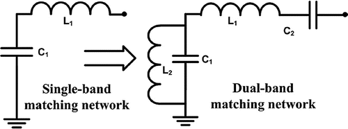
Figure 4. Simulated vs. frequency for different combination of circuit elements.
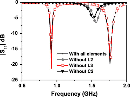
Figure 5. Layout of the proposed dual-band RF energy harvesting circuit.
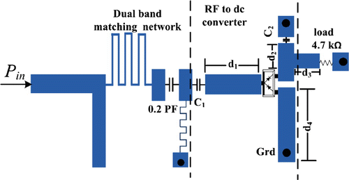
Figure 6. Photograph of the fabricated dual-band RF energy harvesting circuit.
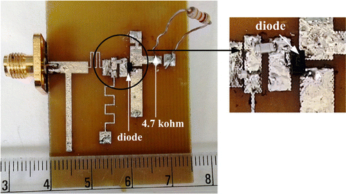
Figure 7. (a) Simulated and measured vs. frequency and (b) measured
for various power levels.
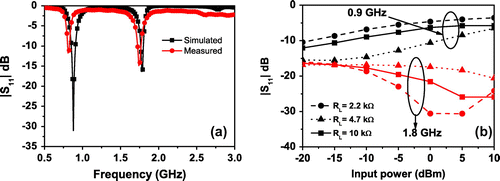
Figure 8. (a) Measured output dc voltage and RF-to-dc conversion efficiency and (b) measured dc voltage vs. frequency.
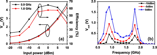
Figure 9. Measured RF-to-dc conversion efficiency for different load impedance.
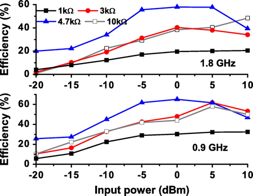
Table 1. Performance comparison of the proposed dual rectifier with recently published works