Figures & data
Table 1. RF and dc magnetron sputtering parameters/process conditions used for Cu1Ga1Se1 and metal film depositions
Figure 1. (A) Representative SEM micrograph (plan view) of a 200-nm thick CuGaSe film deposited by RF sputtered at 600°C from a stoichiometric target (B). Microscopic image of metal contact patterns developed on a CuGaSe thin film: dots separated from infinite area contact by an annular ring space for contact type determination. (C) Si/CGS heterojunction fabrication process flow.
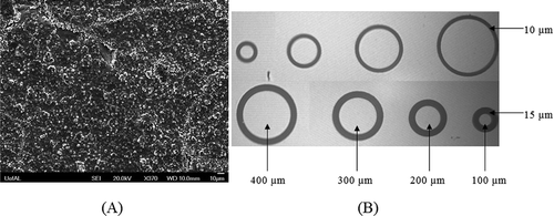
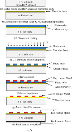
Figure 2. (A) Rutherford backscattering (RBS) spectra from CGS films grown for 90 min at a substrate temperature 600°C. Simulated profiles obtained using “RUMP-RBS Analysis and Simulation” package are shown in red. (B) Bright field transmission electron micrograph and (C) dark field cross-sectional transmission electron micrograph showing the polycrystalline nature of the CGS film. Samples of CuGaSe were deposited at a substrate temperature of 600°C for 90 min.
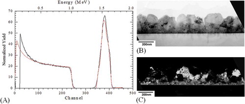
Figure 3. High-resolution TEM micrograph showing the interface between the Si substrate and the CGS film.
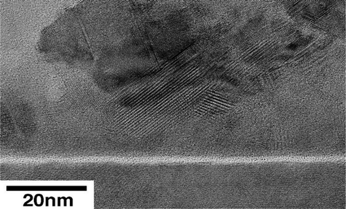
Table 2. Compiled electron diffraction results
Figure 4. Selected area electron diffraction pattern of Si [0 1 1] superimposed on the polycrystalline CGS film.
![Figure 4. Selected area electron diffraction pattern of Si [0 1 1] superimposed on the polycrystalline CGS film.](/cms/asset/41441473-713f-4ffa-a0fe-3e17657cb78a/oaen_a_1514941_f0004_b.gif)
Figure 5. I–V characteristics of 100, 200, 300 and 400 µm ohmic for (A) Cr contact on CGS, (B) Au contact on CGS, (C) Pt contact on CGS and (D) W contact on CGS.
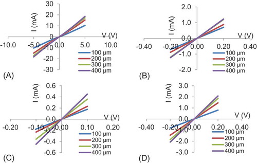
Figure 6. I–V characteristics of 100, 200, 300 and 400 µm: (A) rectifying Ag contacts on CGS and (B) semi-ohmic Mo contacts on CGS.
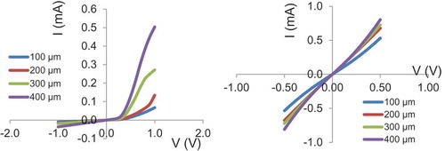
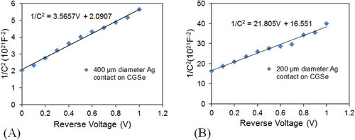
Figure 7. Capacitance–voltage measurements for rectifying Ag circular dots contacts surrounded by infinite area. (A) C–V characteristics for 400 and (B) 200 µm diameter contacts. The doping concentration and built-in potential were estimated from the slope and the intercept on the V-axis, respectively.