
Figures & data
Figure 1. SHE + STT device structure and its switching mechanism for (a) AP to P and (b) P to AP configuration (Barla et al., Citation2021).
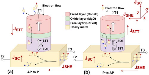
Figure 2. Block diagram of CIM structure, comprising of sense amplifier, logic network with MOS tree, and MTJs. MTJ write circuit is used to change the configuration of MTJs.
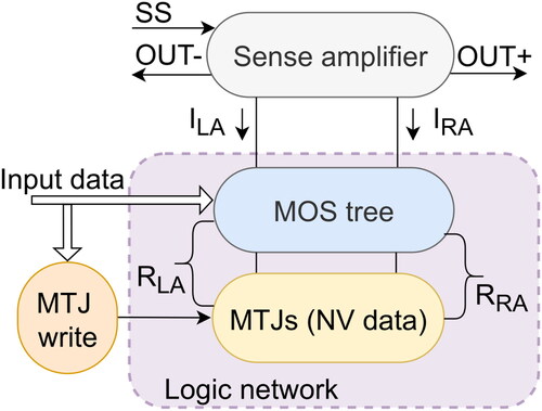
Figure 3. Various sense amplifier circuits developed to read the information stored in the MTJ pair. MTJ0 and MTJ1 are at opposite states. SS (‘0’ or ‘1’) is used to control the mode of operation. Schematic for (a) conventional SRAM based sense amplifier, (b) ten transistors/one capacitor DCM sense amplifier, (c) PCSA, (d) SPCSA, (e) RESPCSA, (f) ISA. Note that these sense amplifiers are developed for STT MTJs. The same sense amplifier circuits can be used for SHE + STT MTJs as their reading mechanism is same.
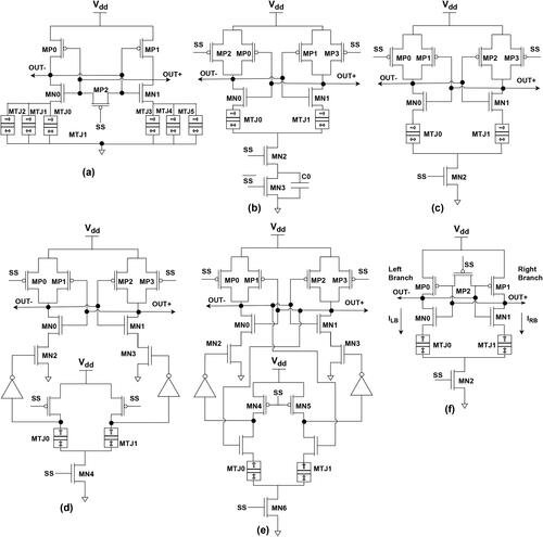
Figure 4. Schematic of AWS write circuitry constituting (a) control circuit, (b) write core and (c) self-termination circuit. Direction of ISTT and ISHE are marked during writing the information bit ‘0’ and ‘1’.
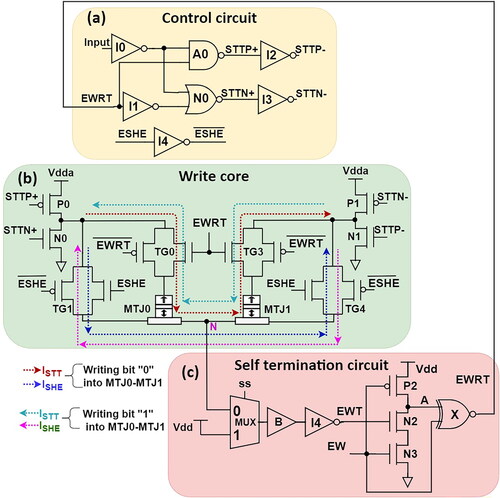
Table 1. Various input signals, intermediate signals, write enabler outputs and the corresponding MTJ states for the AWS circuit.
Figure 5. Hybrid SHE+STT MTJ/CMOS logic gates for CIM structure, showing (a) ISA, (b) MOS tree for: XOR/XNOR, (h) NAND/AND and (g) OR/NOR, (c) logic network, (d) write core, (e) self termination circuit.
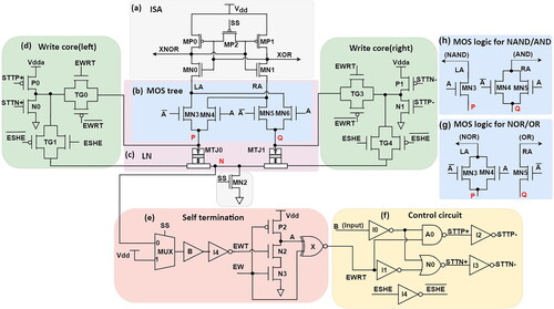
Table 2. Truth table for various logic gates along with the corresponding path resistance for the LA and RA current in logic network.
Table 3. SHE + STT MTJ parameters set during the simulation. Rest of the parameters are retained as mentioned in ref. (Wang et al., Citation2015).
Table 4. Write energy consumption of CW and AWS write circuits.
Figure 6. Waveform for the AWS write circuit showing (a) input (b) write enable (WE), (c) SHE signal (ESHE), (d) state of MTJ0 and (e) MTJ1, (f) node N voltage, output of (g) I4 inverter (EWT) and (h) write completion detector (EWRT),control circuit outputs (i) STTP and (j) STTN, (k) AWS ISTT and (l) conventional ISTT.
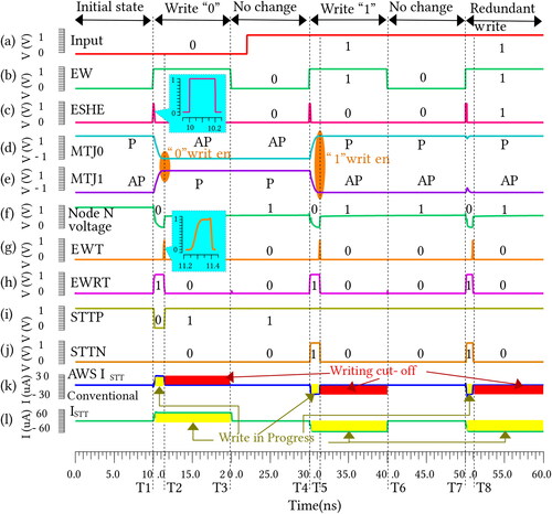
Figure 7. Various input and output waveforms for different hybrid logic gates. Between T1 to T3, one of the condition wherein information bit ‘1’ being written into the MTJ pair is shown. Initially MTJ pair (input B) is stored with information ‘0’. At T1, writing the bit ‘1’ into the MTJ pair was initiated. At time T2, writing the bit ‘1’ is complete. Due to the CM and AWS process, in AWS gates the ISTT current is stopped at T2 whereas in CW gate the ISTT continues to flow till T3. So T3-T2 is the time for which power is saved with ISA + AWS gates. In the pre-charge phase (SS = 0); ISA + AWS gate’s both output and its complement are at Vdd-Vth, whereas for CW gates it is Vdd.
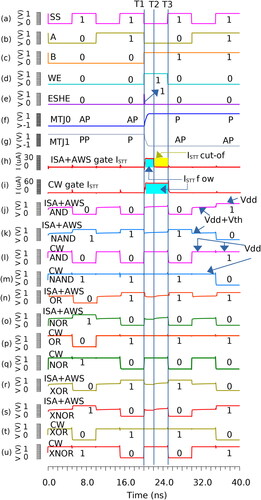
Figure 8. Comparison of (a) read circuitry (b) write circuitry and (c) total (read + write circuitry) power dissipation for CW and ISA + AWS logic gates.
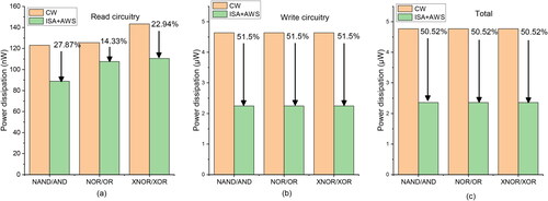
Table 5. Performance comparison between hybrid CW and ISA + AWS logic gates.
Figure 9. Comparison of worst case (a) read and (b) write delay for CW and ISA + AWS logic gates.
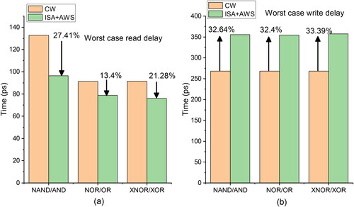
Figure 10. Worst case (a) read and (b) write PDP comparison between CW and ISA + AWS logic gates.
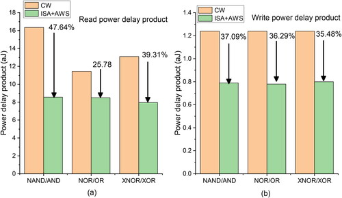
Figure 11. Dependence of read circuitry’s power dissipation, delay and PDP on size of PD transistor for ISA + AWS (a) AND/NAND, (b) OR/NOR, and (c) XOR/XNOR logic gates.
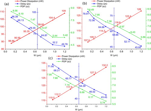
Figure 12. Variation of write circuitry and total power dissipation with the respect to width of the write core transistor.
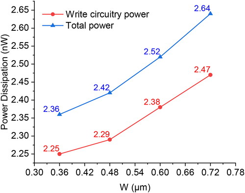
Figure 13. MC simulation showing the power dissipation in CW: AND/NAND (a) LIM circuitry, (b) Write circuitry, (c) total power; OR/NOR (d) LIM circuitry, (e) Write circuitry, (f) total total; XOR/XNOR (g) LIM circuitry, (h) Write circuitry, (i) total power.
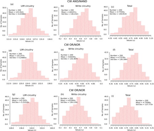
Figure 14. MC simulation showing the power dissipation in ISA + AWS: AND/NAND (a) LIM circuitry, (b) Write circuitry, (c) total power; OR/NOR (d) LIM circuitry, (e) Write circuitry, (f) total total; XOR/XNOR (g) LIM circuitry, (h) Write circuitry, (i) total power.
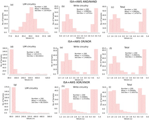
Table 6. MC simulation revealing the various power dissipation for CW and ISA + AWS logic gates with 200 iterations.
interactapasample.tex
Download Latex File (45.4 KB)subfig.sty
Download (21.5 KB)natbib.sty
Download (45.6 KB)interactapasample.bib
Download Bibliographical Database File (12.2 KB)rotating.sty
Download (5.7 KB)booktabs.sty
Download (6.4 KB)epsfig.sty
Download (3.1 KB)interact.cls
Download (24.6 KB)interactapasample.bbl
Download (29.6 KB)Data availability statement
Data available on request from the authors.