Figures & data
Figure 1. Schematic images of the crystal structure of various Bi-chalcogenide compounds. ((a)–(c)) Typical BiS2-based compounds: (a) REOBiCh2 (RE: rare earth or Bi; Ch: S, Se) (Maziopa et al., Citation2014; Mizuguchi, Demura, et al., Citation2012), (b) Eu3F4Bi2Ch4 (Zhai, Zhang, et al., Citation2014; Zhang et al., Citation2015), and (c) Bi4O4SO4Bi2S4 (Mizuguchi, Fujihisa, et al., Citation2012). The electrically conducting layer of these compounds is the two-layer-type Bi2S4 layer. (d) LaOM2S3 (M: Bi, Pb) (Sun et al., Citation2014). The M4S6 conducting layer of LaOM2S3 is similar to the Bi4Te6 layer of (e) CsBi4Te6 (Chung et al., Citation2000).
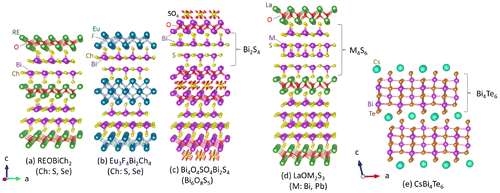
Figure 2. ((a)–(c)) Temperature dependences of (a) electrical resistivity (ρ), (b) Seebeck coefficient (S), and (c) power factor (PF) for LaO1−xFxBiS2. (d) Schematic image of the crystal structure of LaO1−xFxBiS2 and electron doping scenario.
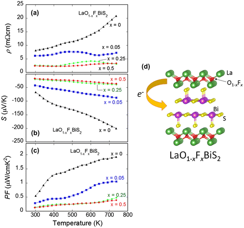
Figure 3. ((a)–(c)) Temperature dependences of (a) electrical resistivity (ρ), (b) Seebeck coefficient (S), and (c) power factor (PF) for LaOBiS2−xSex. (d) Schematic image of the crystal structure of LaOBiS2−xSex and the definitions of the Ch1 and Ch2 sites.
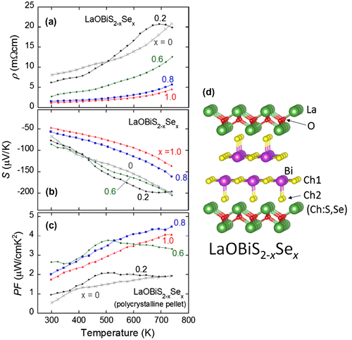
Figure 4. (a) XRD patterns for hot-pressed (HP) LaOBiSSe (x = 1). The Miller indices are shown with the top profile. The asterisk indicates the impurity (La2O3: 7% against the major phase) peak. To investigate the crystal structure anisotropy, XRD measurements were performed for polished pellets with two scattering vectors of P// and P⊥. (b) Schematic image for the definitions of the measurement directions of P// and P⊥ and the hot-pressing direction. ((c)–(f)) Temperature dependences of (c) electrical resistivity (ρ), (d) Seebeck coefficient (S), (e) thermal conductivity (κ), and dimensionless figure-of-merit (ZT) for HP-LaOBiSSe.
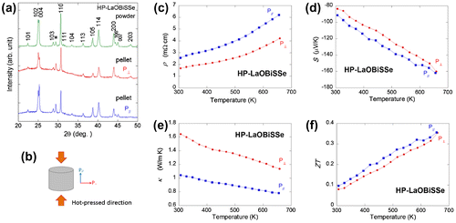
Figure 5. ((a)–(c)) Temperature dependences of (a) electrical resistivity (ρ), Seebeck coefficient (S), and power factor (PF) for CeO1−xFxBiS2. ((d)–(f)) Temperature dependences of (d) ρ, (e) S, and (f) PF for NdO1−xFxBiS2.
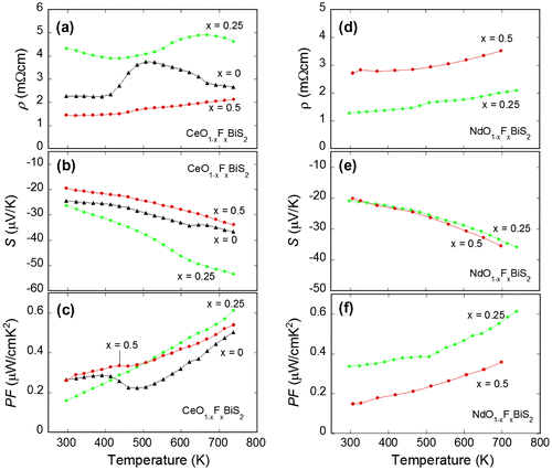
Figure 6. Temperature dependences of (a) electrical resistivity (ρ) and (b) Seebeck coefficient (S) for EuFBiS2. (c) Schematic image of the crystal structure of EuFBiS2.
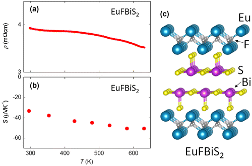
Figure 7. ((a)–(c)) Temperature dependences of (a) electrical resistivity (ρ), Seebeck coefficient (S), and power factor (PF) for LaOBiPbS3. (d) Schematic image of the crystal structure of LaOBiPbS3.
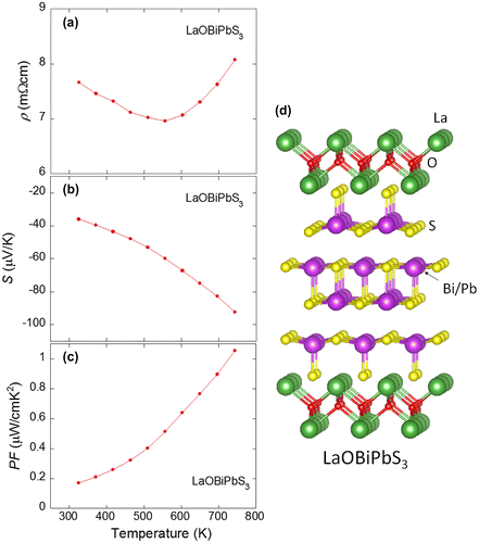
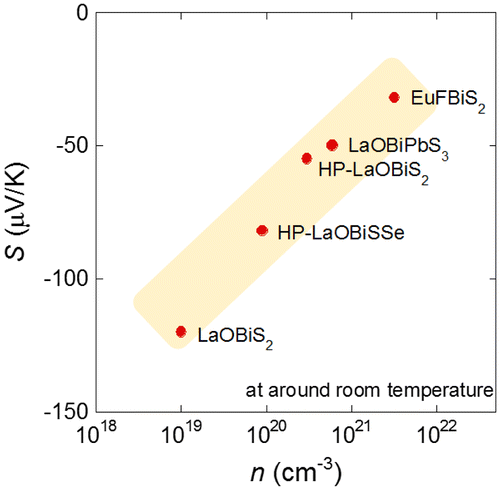
Figure 8. The Seebeck coefficient (S) for several Bi-chalcogenide samples (parent phases) are plotted as a function of the carrier concentration (n) (log scale for n).