Figures & data
Figure 1. (a) The QD-SOA density of states as a function of transition energy. (b) The transition diagram of InAs/InGaAsP/InP QD-SOA.
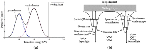
Figure 2. Schematic of a QD-SOA-based Mach–Zehnder Interferometer.
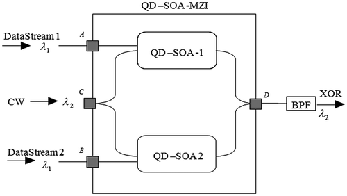
Figure 3. A side-by-side comparison of XOR result for (a) 40 Gb/s and (b) 250 Gb/s XOR operation, insets are the simulated eye diagram of the output wave.
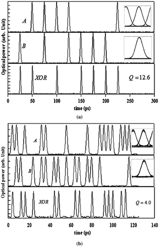
Figure 4. Simulated result for all-optical AND gate operating at 250 Gb/s.
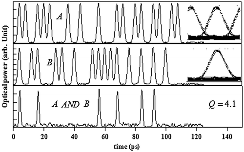
Figure 5. Simulated results for all-optical NOT gate operating at 250 Gb/s.
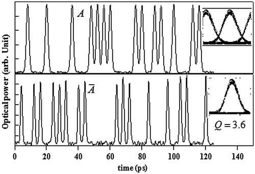
Figure 6. Calculated operation quality factor Q at different pulse width and injected current density, single pulse energy is set to 0.5 pJ. (a) 250 Gb/s XOR operation (b) 160 Gb/s operation.
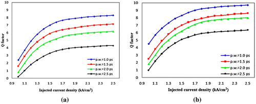
Figure 7. Calculated 250 Gb/s operation quality factor Q at different single pulse energy and transition lifetime from QD excited state to ground state. Injected current density is set to 1.8 kA/cm2. (a) Q factor dependence on single pulse energy (b) Q factor dependence on ES to GS transition lifetime.
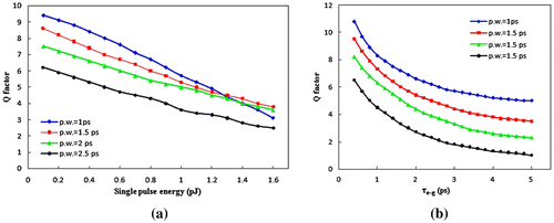
Figure 8. Schematic of the all-optical XOR logic gate, CW: continuous wave.
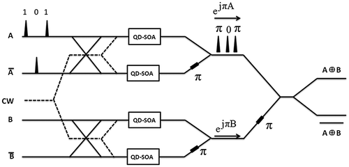
Figure 9. Schematic of the all-optical AND and NAND logic gates, CW: continuous wave.
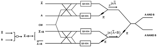
Figure 10. Data A and Data B are shown on the top. Simulated results of output (XOR) and eye diagram of the output are shown below.
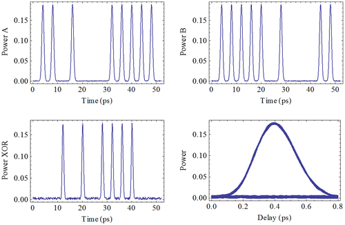
Figure 11. Data A and Data B are shown on the top. Simulated results of output (AND) and eye diagram of the output are shown below.
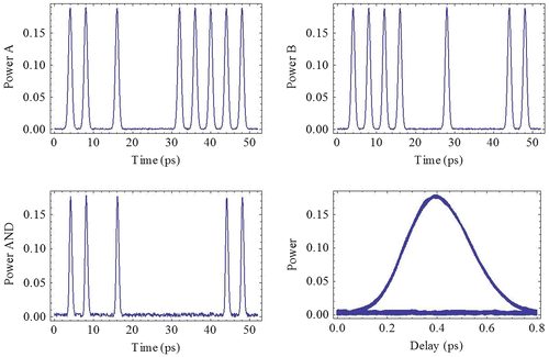
Figure 12. Data A and Data B are shown on the top. Simulated results of output (NAND) and eye diagram of the output are shown below.
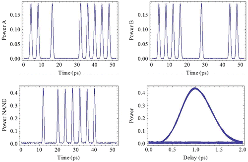
Figure 13. The left figure is the schematic of the Set-Reset Latch. The right figure is the truth table for the Set-Reset function.
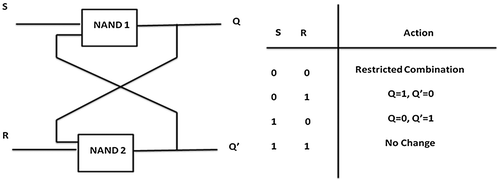
Figure 14. The left figure is the schematic of the D-Flip-Flop. The right figure is the truth table for D-Flip-Flop function.
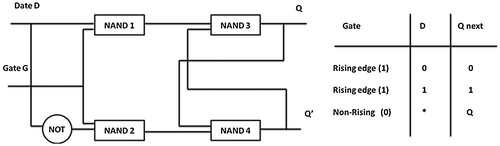
Figure 15. Schematic of all-optical NAND logic gate based on QD-SOA-MZI.
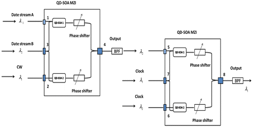
Figure 16. Data A and Data B are shown in the left. Simulated results of output (NAND) and eye pattern of the output are shown in the right.
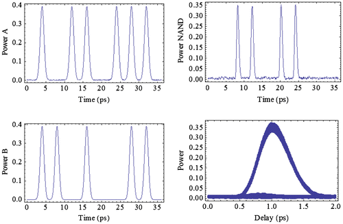
Figure 17. Set and Reset are shown in the left. Simulated results of output (Q) and eye pattern of the output are shown in the right.
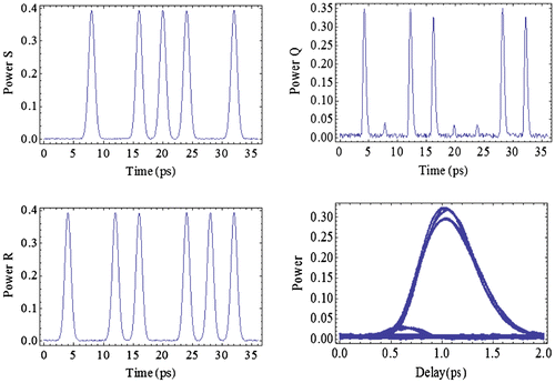
Figure 18. Data and Gate are shown in the left. Simulated results of output (Q) and eye pattern of the output are shown in the right.
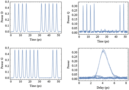
Figure 19. The left figure is the schematic of encryption. The right figure is the schematic of decryption.
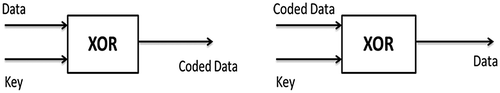
Figure 20. Design of PRBS generator. (a): Block diagram of a LFSR (b): functional unit, including two QD-SOA MZIs operating as XOR and AND gates.
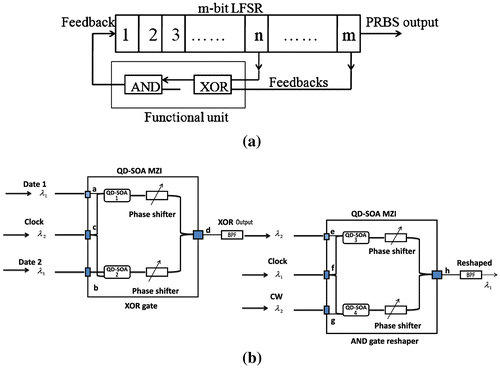
Figure 21. Block diagram of cascaded designed key-stream generator.
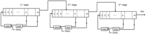
Figure 22. Block diagram of parallel designed key-stream generator.
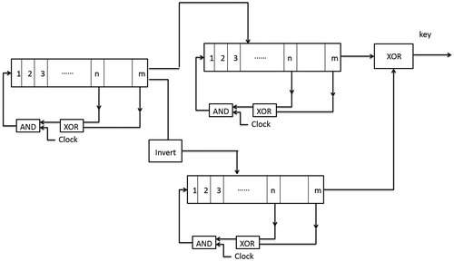
Figure 23. Input data is shown at the top-right corner and key is shown at the top-left corner. Simulated results of encrypted data and decrypted data are shown at the bottom-left corner and bottom-right corner, respectively.
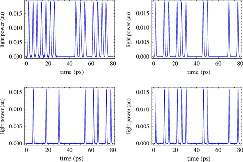
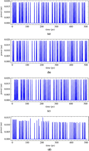
Figure 24. Simulation result of PRBS sequences generated by 7-bit LFSR, operating at 250 Gb/s.
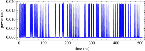
Figure 25. (a) Simulation result of the first stage in cascaded design, input is seven “1”; (b) Simulation result of the second stage in cascaded design, input is “8th–14th” of the output of the first stage; (c) Simulation result of the third stage in cascaded design, input is “15th–21st” of the output of the second stage.
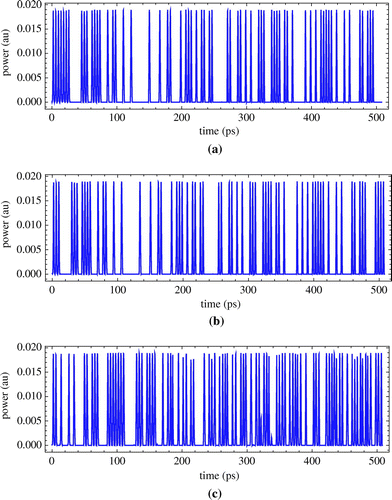
Figure 26. (a) Simulation result of the first LFSR in parallel design, input is seven “1”; (b) Simulation result of the second LFSR in parallel design, input is “8th-14th” of the output of the first LFSR; (c) Simulation result of the third LFSR in parallel design, input is the invert of “8th–14th” of the output of the first LFSR; (d) the final output of parallel design: XOR of the output of second and third LFSR.