
Figures & data
Figure 1. Schematic illustration of different types of representative materials. (a) Direct bandgap semiconductor. (b) Indirect bandgap semiconductor. (c) Topological insulators. (d) Semimetal with valance band and conduction band touching. (e) Semimetal with valance band and conduction band overlapping in different momentum point. (f) Topological semimetal owns linear energy dispersion in the bulk. (g) Topological semimetal has additional hole pockets near the Weyl point.
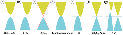
Figure 2. The negative magnetoresistance in Dirac semimetals. (a) The Dirac cone shift under an external magnetic field in Dirac semimetal Na3Bi [Citation94]. When an external magnetic field is applied, the degenerate Dirac point will split into two Weyl nodes along the magnetic field direction in the momentum space. Thus a Dirac semimetal is transformed into a Weyl semimetal. (b) The chiral anomaly effect [Citation94]. When the magnetic field is parallel to the electric field, the chiral anomaly effect occurs, rendering the charge imbalance between the two Weyl nodes. Thus a chiral current happens, leading to an additional electric conductivity and the observed negative magnetoresistance. (c) The angle dependent experiment of magnetotransport [Citation94]. Apparently the negative magnetoresistance decreases with the magnetic field direction deviating from the electric field direction and finally disappears when the magnetic field is perpendicular to the electric field. (d) Dirac semimetal Cd3As2 [Citation104]. The resistance–temperature (R–T) curve shows a typical low-carrier density behavior. (e) The negative magnetoresistance at different temperature [Citation104]. (f) The chiral anomaly-induced thermal power suppression effect [Citation132].
![Figure 2. The negative magnetoresistance in Dirac semimetals. (a) The Dirac cone shift under an external magnetic field in Dirac semimetal Na3Bi [Citation94]. When an external magnetic field is applied, the degenerate Dirac point will split into two Weyl nodes along the magnetic field direction in the momentum space. Thus a Dirac semimetal is transformed into a Weyl semimetal. (b) The chiral anomaly effect [Citation94]. When the magnetic field is parallel to the electric field, the chiral anomaly effect occurs, rendering the charge imbalance between the two Weyl nodes. Thus a chiral current happens, leading to an additional electric conductivity and the observed negative magnetoresistance. (c) The angle dependent experiment of magnetotransport [Citation94]. Apparently the negative magnetoresistance decreases with the magnetic field direction deviating from the electric field direction and finally disappears when the magnetic field is perpendicular to the electric field. (d) Dirac semimetal Cd3As2 [Citation104]. The resistance–temperature (R–T) curve shows a typical low-carrier density behavior. (e) The negative magnetoresistance at different temperature [Citation104]. (f) The chiral anomaly-induced thermal power suppression effect [Citation132].](/cms/asset/ae6ab332-1b3c-4148-9755-a7656d37a29f/tapx_a_1327329_f0002_oc.gif)
Figure 3. The surface states mediated transport experiment. (a) Cd3As2 microplates with different thickness [Citation144]. (b) The theoretical model, namely ‘Weyl orbit’ [Citation143], which weaves together the chiral states in the bulk with the topological Fermi arc states on opposite surfaces in a closed orbit. Moreover, when the carriers are tunneling from the bulk state to the surface state, namely Fermi arc, an additional oscillation frequency will be induced. (c) An additional oscillation frequency is observed when the magnetic field is perpendicular to the microplate plane [Citation144]. denotes that the magnetic field direction is parallel to the normal direction of the microplate. (d) The standard four-terminal measurement of Cd3As2 nanowire with an axial magnetic field applied [Citation153]. (e) AB effect in Cd3As2 nanowire [Citation153]. A typical periodic oscillation is observed and the amplitude is gradually decreasing with temperature increasing. (f) The AAS effect in Cd3As2 nanowire with diameter
[Citation153].
![Figure 3. The surface states mediated transport experiment. (a) Cd3As2 microplates with different thickness [Citation144]. (b) The theoretical model, namely ‘Weyl orbit’ [Citation143], which weaves together the chiral states in the bulk with the topological Fermi arc states on opposite surfaces in a closed orbit. Moreover, when the carriers are tunneling from the bulk state to the surface state, namely Fermi arc, an additional oscillation frequency will be induced. (c) An additional oscillation frequency is observed when the magnetic field is perpendicular to the microplate plane [Citation144]. denotes that the magnetic field direction is parallel to the normal direction of the microplate. (d) The standard four-terminal measurement of Cd3As2 nanowire with an axial magnetic field applied [Citation153]. (e) AB effect in Cd3As2 nanowire [Citation153]. A typical periodic oscillation is observed and the amplitude is gradually decreasing with temperature increasing. (f) The AAS effect in Cd3As2 nanowire with diameter [Citation153].](/cms/asset/f3d0ca86-14a7-430a-8656-3a805657a525/tapx_a_1327329_f0003_oc.gif)
Figure 4. Point contact-induced superconductivity in Dirac semimetals. (a) A typical device for point contact measurement [Citation196]. The R–T transition is observed. (b) Normalized dI/dV spectra at different temperatures varying from 0.28 to 3.8 K without an external magnetic field [Citation196]. A zero bias conductance peak and double conductance peaks are observed. (c) In the thermal regime, the dV/dI spectra show a resistance dip (or conductance peak) due to superconductivity and double resistance peaks due to critical field effect [Citation197]. (d) In the ballistic regime, the double conductance peaks demonstrate an energy gap up to 13 K and the zero bias conductance peak is observed [Citation197].
![Figure 4. Point contact-induced superconductivity in Dirac semimetals. (a) A typical device for point contact measurement [Citation196]. The R–T transition is observed. (b) Normalized dI/dV spectra at different temperatures varying from 0.28 to 3.8 K without an external magnetic field [Citation196]. A zero bias conductance peak and double conductance peaks are observed. (c) In the thermal regime, the dV/dI spectra show a resistance dip (or conductance peak) due to superconductivity and double resistance peaks due to critical field effect [Citation197]. (d) In the ballistic regime, the double conductance peaks demonstrate an energy gap up to 13 K and the zero bias conductance peak is observed [Citation197].](/cms/asset/8dae4f1d-2139-4f67-b4c5-440b9ffb2fef/tapx_a_1327329_f0004_oc.gif)