
Figures & data
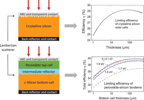
Figure 1. Schematic geometry of (a) a solar cell with a single layer leading to single-pass absorption or (b) a layer with a Lambertian scatterer in the front and a back reflector in the rear side, leading to Lambertian light trapping; (c) short-circuit current density for c-Si, a-Si:H, GaAs, and CIGS (taking
) as a function of thickness, under AM1.5 solar spectrum. Dashed lines refer to the single-pass case, while solid lines refer to the Lambertian limit with
, as defined in Ref. [Citation18]. Reflection losses are neglected throughout. Notice that the silicon curves differ from those published in Ref. [Citation23], due to the use of different data for c-Si [Citation19,Citation24] and for a-Si:H [Citation20].
![Figure 1. Schematic geometry of (a) a solar cell with a single layer leading to single-pass absorption or (b) a layer with a Lambertian scatterer in the front and a back reflector in the rear side, leading to Lambertian light trapping; (c) short-circuit current density Jsc for c-Si, a-Si:H, GaAs, and CIGS (taking x=0.08) as a function of thickness, under AM1.5 solar spectrum. Dashed lines refer to the single-pass case, while solid lines refer to the Lambertian limit with Rb=1, as defined in Ref. [Citation18]. Reflection losses are neglected throughout. Notice that the silicon curves differ from those published in Ref. [Citation23], due to the use of different data for c-Si [Citation19,Citation24] and for a-Si:H [Citation20].](/cms/asset/17323ce6-5ce7-4491-a2c0-0802e01ebd83/tapx_a_1548305_f0001_oc.jpg)
Figure 2. (a) Photogeneration profile of a 10-µm thick c-Si solar cell with Gaussian disorder, described by the RMS deviation of height nm and the lateral correlation length lc = 160 nm. The whole cell is shown in the inset, while the main plot shows the photogeneration profile close to the texture. All lengths are in µm. Reprinted from Ref. [Citation87], with the permission of AIP Publishing. (b) Structure considered in the FEM simulations. The p-n junction is made of an 80-nm thick n-type layer with donor concentration Nd = 1019 cm−3, and a p-type layer of thickness d−80 nm with acceptor concentration Na = 1016 cm−3. The ARC and silver layers serve as front and back contacts, respectively.
![Figure 2. (a) Photogeneration profile of a 10-µm thick c-Si solar cell with Gaussian disorder, described by the RMS deviation of height σ=300 nm and the lateral correlation length lc = 160 nm. The whole cell is shown in the inset, while the main plot shows the photogeneration profile close to the texture. All lengths are in µm. Reprinted from Ref. [Citation87], with the permission of AIP Publishing. (b) Structure considered in the FEM simulations. The p-n junction is made of an 80-nm thick n-type layer with donor concentration Nd = 1019 cm−3, and a p-type layer of thickness d−80 nm with acceptor concentration Na = 1016 cm−3. The ARC and silver layers serve as front and back contacts, respectively.](/cms/asset/436f28b7-c2c2-454b-8763-e1702188c977/tapx_a_1548305_f0002_oc.jpg)
Figure 3. The main electrical parameters for c-Si solar cells without surface recombination: (a) open-circuit voltage and short-circuit current density
, (b) fill factor FF and conversion efficiency η. The diffusion lengths related to SRH recombination are LB = 232 µm for electrons in the p-type base [Citation90], and LE = 23.2 µm for holes in the n-type emitter [Citation25].
![Figure 3. The main electrical parameters for c-Si solar cells without surface recombination: (a) open-circuit voltage Voc and short-circuit current density Jsc, (b) fill factor FF and conversion efficiency η. The diffusion lengths related to SRH recombination are LB = 232 µm for electrons in the p-type base [Citation90], and LE = 23.2 µm for holes in the n-type emitter [Citation25].](/cms/asset/3e66e045-cf46-4575-86df-02b98a3fd7f4/tapx_a_1548305_f0003_oc.jpg)
Figure 4. (a) Energy conversion efficiency for solar cells with perfect surface passivation (SB = SE = 0 cm/s) as a function of the electron diffusion length in the base (with LE = 23.2 µm) and of the cell thickness. The optimal configurations lie along the blue solid line with symbols. (b) Energy conversion efficiency as a function of the back surface recombination velocity
and of the cell thickness for LB = 232 µm, LE = 23.2 µm, and SE = 103 cm/s. All results are calculated by the FEM. Reprinted (with adaptation) from Ref. [Citation88], with permission from Elsevier.
![Figure 4. (a) Energy conversion efficiency for solar cells with perfect surface passivation (SB = SE = 0 cm/s) as a function of the electron diffusion length in the base LB (with LE = 23.2 µm) and of the cell thickness. The optimal configurations lie along the blue solid line with symbols. (b) Energy conversion efficiency as a function of the back surface recombination velocity SB and of the cell thickness for LB = 232 µm, LE = 23.2 µm, and SE = 103 cm/s. All results are calculated by the FEM. Reprinted (with adaptation) from Ref. [Citation88], with permission from Elsevier.](/cms/asset/428c05f5-4c6e-4c30-a8a6-656674a308c5/tapx_a_1548305_f0004_oc.jpg)
Figure 5. (a) Scheme of the p-n junction for the generalized Hovel model. The impurity charges in the space charge region correspond to an n-emitter, p-base configuration, although the formulation of the model applies to both n-p and p-n configurations. The emitter is usually more narrow and highly doped than the base. (b) Scheme of the solar cell structure for the three models, including front and back contacts (serving also as ARC and back reflector, respectively) and the Lambertian scattering layer.
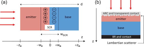
Figure 6. (a) Short-circuit current density , (b) open-circuit voltage
, (c) fill factor FF, and (d) efficiency
as a function of the absorber thickness. Results are calculated with the diode equation model (red lines), with the generalized Hovel model (blue dotted lines), and by the FEM method (black solid lines). We include only intrinsic Auger recombination, and assume no Shockley–Read–Hall or surface recombination. The triangles indicate the parameters of the record silicon solar cell with 26.3% efficiency [Citation6]. Reproduced (with adaptation) from Ref. [Citation98], with permission from IOP Publishing.
![Figure 6. (a) Short-circuit current density Jsc, (b) open-circuit voltage Voc, (c) fill factor FF, and (d) efficiency η as a function of the absorber thickness. Results are calculated with the diode equation model (red lines), with the generalized Hovel model (blue dotted lines), and by the FEM method (black solid lines). We include only intrinsic Auger recombination, and assume no Shockley–Read–Hall or surface recombination. The triangles indicate the parameters of the record silicon solar cell with 26.3% efficiency [Citation6]. Reproduced (with adaptation) from Ref. [Citation98], with permission from IOP Publishing.](/cms/asset/6ce2c3c5-b43e-472e-ad11-be1d898ef974/tapx_a_1548305_f0006_oc.jpg)
Figure 7. Effect of Shockley–Read–Hall recombination, expressed by the diffusion length, , for different absorber thicknesses. Other parameters are the same as in . Results are calculated with the generalized Hovel model.
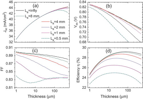
Figure 8. Effect of surface recombination, expressed by the surface recombination velocity at the rear surface, for different absorber thicknesses. Other parameters are the same as in . Results are calculated with the finite-element method.
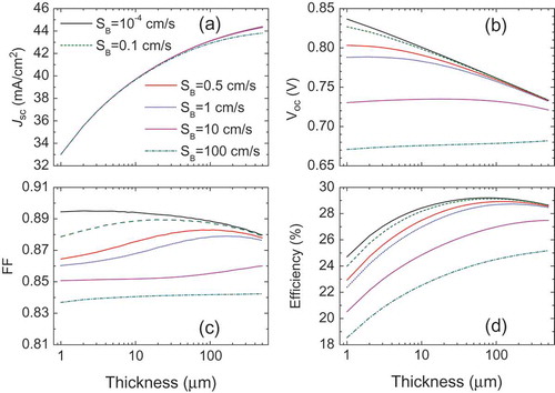
Figure 9. (a) Scheme of the silicon/perovskite tandem solar cell. (b) Efficiency of the tandem as a function of the thickness of the silicon bottom cell, calculated for different values of the perovskite bandgap. Adapted from Ref. [Citation98], with permission from IOP Publishing. Inset: maximum efficiency as a function of perovskite gap.
![Figure 9. (a) Scheme of the silicon/perovskite tandem solar cell. (b) Efficiency of the tandem as a function of the thickness of the silicon bottom cell, calculated for different values of the perovskite bandgap. Adapted from Ref. [Citation98], with permission from IOP Publishing. Inset: maximum efficiency as a function of perovskite gap.](/cms/asset/ee79168f-96c0-4a2e-b5d1-f590d160a104/tapx_a_1548305_f0009_oc.jpg)