Figures & data
Figure 1. (a) Molecular structure of PTCDA. (b) Large-scale STM image showing a monolayer SAMN of PTCDA on EG-SiC. (c) High-resolution STM image showing a continuous PTCDA layer over a step edge. Adapted with permission from ref. 32. Copyright © 2009 Nature Publishing Group (d) and (e) Molecular self-assembly of PTCDA on bilayer graphene. (f) STS spectra on pristine bilayer graphene compared with STS spectra on a region close to a PTCDA layer, showing a shift of 75 mV caused by charge transfer. Adapted with permission from ref. 34. Copyright © 2008 Wiley-VCH.
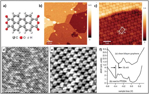
Figure 2. (a) and (b) chemical structure of ODA and NCA molecules, respectively. (c) and (d) show AFM topographical images of ODA and NCA self-assembled on HOPG. (e) and (f) show AFM topographic images of ODA and NCA molecules self-assembled on CVD graphene. The lamellar structure of molecules is clearly observed in these images on both substrates. (g) Typical Raman spectra of CVD grown graphene before and after deposition of ODA and NCA. (h) Transfer characteristics of devices before and after functionalization with ODA and NCA via dip coating. (i) Transfer characteristics of devices doped and after dopant removal. (j) Transfer characteristics after doping by drop casting. Adapted with permission from ref 44. Copyright © 2016 The Royal Society of Chemistry.
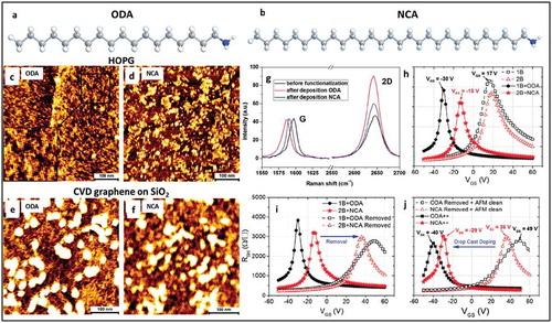
Figure 3. (a) Schematic representation of SAMN monolayers formed by spiropyran derivatives on MoS2, undergoing photo-induced isomerization, leading to a structural rearrangement. Black arrows indicate the molecular dipoles, which align upon photo-induced isomerization. N1s core level spectra of SP molecules coated on HOPG when kept in the dark (b) after UV-irradiation (c) and after irradiation by green light (d), show different N hybridization states in agreement with the schematic in (a). High-resolution STM images of SP molecules on HOPG after spin coating (e) after UV irradiation (f) and) 48 h after UV-irradiation (g), showing molecular ordering upon UV irradiation. Adapted with permission from ref 47. Copyright © 2018 Nature Publishing Group.
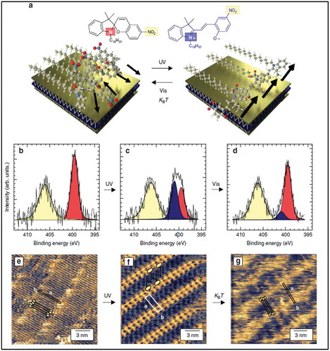
Figure 4. (a1-d1) AFM topographic images of MoS2 flakes and (a2-d2) KPFM surface potential maps corresponding to the areas sown in a1-d1. (a3-d3) show the corresponding surface profiles. Adapted with permission from ref 53. Copyright © 2013 American Chemical Society.
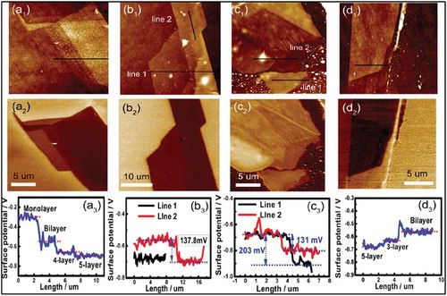
Figure 5. (a) Schematic of a diazo gated sample in trans and in the cis state. (b) Series of the PL intensity recorded from the MoS2-mSAM after UV exposure, irradiating the sample for the different duration and switching back to trans state after 120 min of white light exposure. (c) PL spectra showing switching from trans to cis and back to trans states (d) AFM (left) and KPFM (right) measurements recorded from multilayer MoS2-mSAM-Cl and (e) from multilayers MoS2-mSAM samples in trans state. Adapted with permission from ref 58. Copyright © 2014 American Institute of Physics.
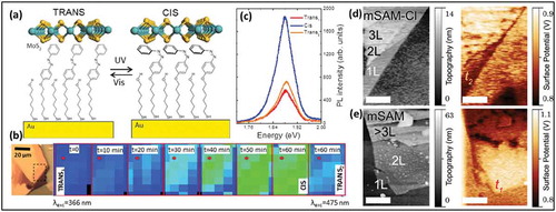
Figure 6. AFM images of an oleylamine functionalized MoS2 flake (and d) and the corresponding height profile (b). (c) shows Raman spectra before and after functionalization of the MoS2 by oleylamine molecules. A tentative model of self-assembled oleylamine molecules is shown in (e). Transport characteristics before doping, after doping and after removal of OA doping are compared in f. Adapted with permission from ref 59. Copyright ©2016 American Institute of Physics.
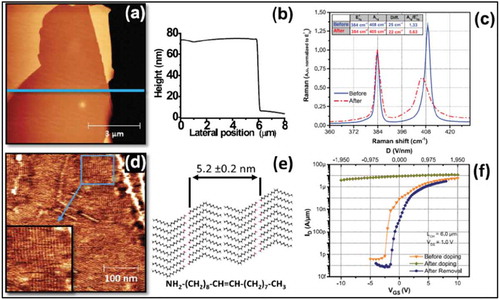
Figure 7. (a) Surface topography of F4-TCNQ functionalized MoS2, showing island-like F4-TCNQ particles with an average height around 20 nm. (b) Surface potential distribution of the same area as in a), the dark areas correspond to F4-TCNQ island sites. (c) and (d) show surface topography and potential distribution, respectively, after annealing the samples, (e) shows cross-section profile of the lines marked in (c) and (d). (f) Schematic of space charge region in F4-TCNQ molecules. Adapted with permission from ref 62. Copyright © 2018 Wiley-VCH.
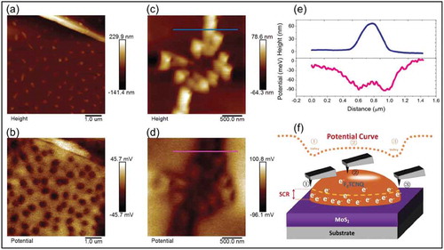
Figure 8. (a) and (b) STM images of CoPc self-assembly in the low coverage regime with one molecule per moiré unit cell. (c) and (d) Higher coverage results in filling the wires with locally square-packed regions. The image in panel d corresponds to the area marked by the red rectangle in panel c. (e) STS Spectra measured on CoPC adsorbed in the wire region of the moiré unit cell; red solid line is measured on the metal center and orange-dashed line on the carbon backbone. (f) STS spectra measured on a molecule adsorbed in the pore region of the moiré unit cell; the dark blue solid line is the metal center and dashed light blue the carbon backbone. Adapted with permission from ref 65. Copyright © 2013 American Chemical Society.
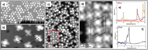
Figure 9. (a) Effect of NMP passivation compared to an inert solvent (THF) and a pristine sample on ca. five nm thick flakes with the comparable area. (b) Influence of thickness on the degradation of NMP-protected flakes stored in darkness, clearly surpassing 25 days of stability. (c) Influence of continuous visible light illumination on 5 and 9 nm thick flakes. (d) AFM images showing a 9 nm flake protected with NMP after 2, 8, and 20 days under ambient conditions. Adapted with permission from ref 67. Copyright © 2017 American Chemical Society.
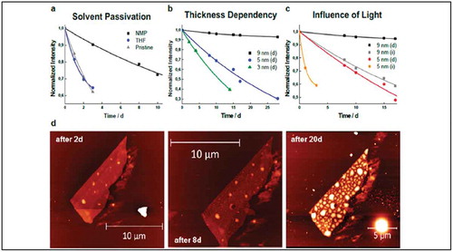
Figure 10. High-resolution AFM images of CA.M deposited on BP (a). Arrows indicate the direction of the principal axis of the CA.M structure, which is aligned with the BP rows. The inset shows the underlying BP.(b) A schematic of melamine, cyanuric acid and the CA.M complex (c) A high-resolution AFM image with individually resolved molecules. (d-e) Optical micrographs and (g-h)XPS spectra taken illustrating the passivation of BP by CA.M by comparing non-passivated BP exposed to ambient conditions (d and g) BP passivated with CA.M (e and h). Adapted with Permission from ref 68. Copyright © 2017 Nature Publishing Group.
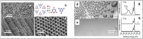
Figure 11. (a) Schematic showing the spontaneous reduction of p-nitrobenzene diazonium (NBD) and its reaction with graphene, leading to covalent attachment of aryl groups to graphene Adapted with permission from ref 86 Copyright © 2011 American Chemical Society. (b) ARPES measurements of NBD-functionalized graphene showing the band structure perpendicular to the Γ-K direction at the graphene K-point (incident photon energy is 36 eV). Two diffuse bands representing gapped Dirac cones are visible. (c) Changes in the Raman spectra in exfoliated and epitaxial graphene due to NBD-functionalization, ID/IG = 3.3. d and (e) Comparison of AFM images of pristine EG and NBD-EG, respectively. Adapted with permission from ref 10. Copyright © 2010 American Chemical Society.
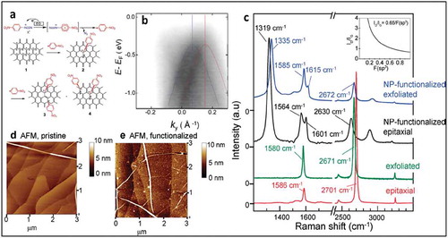
Figure 12. (a) STM image of the chemically modified graphene surface preceding nanopatterning. (b) STM image following bias-dependent nanopatterning of three horizontal lines at a constant tunneling current (1.0 nA) and tip velocity (100 Å/s). (c) Additional nanopatterning of three vertical lines, showing linewidths at the sub-5 nm length scale. All STM images were acquired at a sample bias of +1.85 V and tunneling current of 0.06 nA. Adapted with permission from ref 87. Copyright ©2010 American Chemical Society. STM images of clusters after grafting from a 1 mM solution of (f) 4-NBD and (g) 3,5-TBD on CVD graphene on Cu, (h) The Raman spectra showing strong D peak at 1332 cm−1, confirms grafting of diazonium molecules. Adapted with permission from ref 12. Copyright © 2015 American Chemical Society.
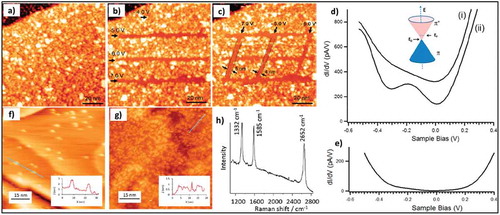
Figure 13. (a) STM image of DBT molecules assembled on HOPG, the schematic on the image shows possible molecular packing. STM height (b) and current (c) images of DBT molecules assembled on graphene show a similar contrast. d) Raman spectra of graphene/SiO2 substrate after spin coating of DBT (0.5 mM in CHCl3), electrochemical grafting, and washing. Adapted with permission from 89 Copyright © 2016 American Chemical Society. e) An illustration for an EC cell contains a solution double layer consisting of an aqueous phase containing diazonium molecules (light blue) and an organic templating phase(red). f) A schematic representation for linear grafting through the self-assembled molecular network of alkane template (g-j) STM images of functionalized samples showing a linear pattern of the grafted molecules, obtained by using pentacontane (g), tetracontane (h), and triacontane (i) in tetradecane as templates. Adapted with permission from 90. Copyright © 2018 American Chemical Society.
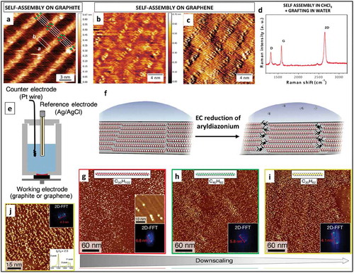
Figure 14. (a) Atomic-resolved STM image of the (6√36√3)R30 reconstruction of the SLG epitaxially grown on SiC(0001) (b) STM image of single atom vacancies formed upon argon irradiation on the surface (c) STM image obtained after dosing the vacancies with 4L of p-AP; (d)Top and side views of the optimized model for a single-vacancy created within a SLG on a graphene buffer layer and top and side views of the optimized geometry of a doubly dehydrogenated p-AP molecule with the nitrogen atom integrated within a monovacancy in the SLG lattice (e) N 1s core level spectra after p-AP grafting on a SLG surface without and with atomic vacancies. (f) ARPES spectra of a p-AP functionalized SLG. Cut along kx direction. Adapted with permission from ref 91. Copyright © 2017 Nature Publishing group.
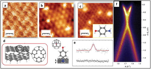
Figure 15. (a) STM image of FePc on graphene islands on Ir(111) showing FePC molecules in different-lobed states. Inset: Zoom-on four-lobe FePc dimer overlaid with the molecular structure. (b) dI/dV spectra obtained at the center of the four-lobe (blue) and three-lobe (red) species. (c) Large-scale STM image of three-lobe FePc molecules on graphene on Ir(111) with superimposed red lines showing the moiré lattice. The positions of the missing lobes of the molecules are indicated by white dots. Adapted with Permission from ref 92. Copyright © 2015 American Chemical Society (d) STM image of F4TCNQ molecules adsorbed on G/Ir(111) surface. Most of the molecules are in the two-legged configuration; one molecule in flat geometry is highlighted by a black circle. The moiré unit cell is indicated by the black parallelogram. The black dots indicate the corners (fcc sites) of the moiré pattern. (e) Illustration of the G/Ir(111) moiré unit cell depicting different registries between the carbon atoms and the underlying Ir substrate. (f) STM topography image showing the two-legged and flat adsorption geometries with respect to the G/Ir(111) moiré. The fcc and hcp regions have been depicted by filled and open circles. Adapted with permission from ref 93. Copyright © 2017 American Chemical Society.
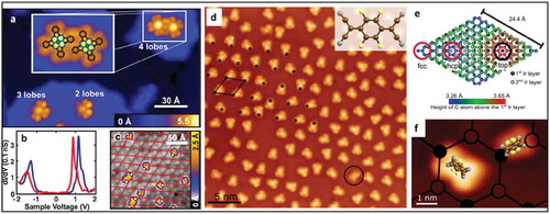
Figure 16. (a) Schematic illustrations of the functionalization of MoS2 by 4-NBD molecules (b) AFM images at a different reaction time of NBD grafting on pristine MoS2 flakes compared to Ar plasma treated MoS2 flakes. (c) optical microscope image of MoS2 flakes showing different layer thicknesses. (d) AFM image of the marked area in (c), (e-h) PL spectra and PL intensity map of the functionalized MoS2 flake from (c) Adapted with permission from 27. Copyright © 2018 American Chemical Society.
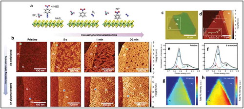
Figure 17. (a,b) AFM images of 4-layer MoS2 after thermal annealing on a SiO2/Si substrate. (c,d) AFM images of the same MoS2 samples after the doping process using MEA and FDT, respectively. The surface roughness of each sample was calculated using these AFM images collected from the blue circle (substrate) and yellow circle (MoS2 surface). PL spectra of functionalized MoS2 before and after doping process; (e) n-doping phenomenon (MEA), (f) p-doping phenomenon (FDT). Adapted with permission from ref 22. Copyright © 2015 American Chemical Society.
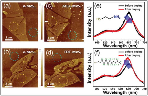
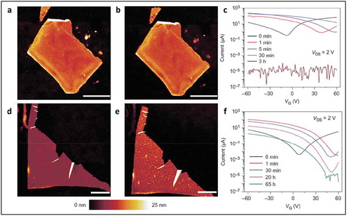
Figure 18. AFM characterization of BP morphology before and after ambient exposure. (a) BP flake immediately after functionalization with 10 mM 4-NBD for 30 min. (b) The same flake as in a after 10 days of ambient exposure. (d) Pristine BP flake immediately after exfoliation. (e) The same flake as in d after 10 days of ambient exposure has distinct morphological protrusions indicative of chemical degradation. (c) Transfer curves for an exfoliated BP FET as a function of exposure time to 10 mM 4-NBD demonstrate strong p-type doping and show a loss of conduction. VDS, drain-source voltage. (f) Transfer curves for an exfoliated BP FET as a function of exposure time to 1 μM 4-NBD. Adapted with permission from ref 105. Copyright © 2016 Nature Publishing Group.