
Figures & data
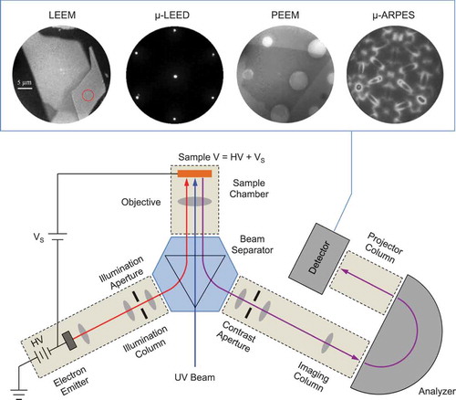
Figure 1. (a) Schematic of the Elmitec LEEM/PEEM system used for much of the SPE-LEEM studies presented here. The sample is illuminated by the incident electron beam generated from an electron emitter, deflected by the beam separator. The electrons are decelerated by the cathode lens and focused on the sample surface by an objective. The reflected electrons are reaccelerated and deflected to the imaging column. (b–e) Different imaging modes that highlight different features of the surface. Reproduced with permissions of Ref [Citation60,Citation145].
![Figure 1. (a) Schematic of the Elmitec LEEM/PEEM system used for much of the SPE-LEEM studies presented here. The sample is illuminated by the incident electron beam generated from an electron emitter, deflected by the beam separator. The electrons are decelerated by the cathode lens and focused on the sample surface by an objective. The reflected electrons are reaccelerated and deflected to the imaging column. (b–e) Different imaging modes that highlight different features of the surface. Reproduced with permissions of Ref [Citation60,Citation145].](/cms/asset/4dceace0-55c9-4d7e-ab25-6dd1b54306ab/tapx_a_1688187_f0001_oc.jpg)
Figure 2. (a) Electronic structure of bulk MoS2 constructed in (,
,
) space one obtained by stacking constant-energy maps. (b) An ARPES band map along the
high symmetry direction as denoted by a vertical slide in (a).
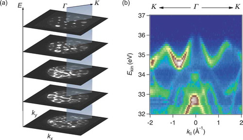
Figure 3. (a) Schematic of the three steps of the multiple scattering in dynamical LEED calculations, i.e. scattering of electrons by a single atom (left), an atomic plane (middle), and the bulk crystal (right). (b) Workflow of the self-consistent structural optimization.
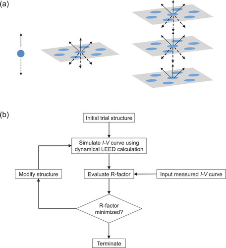
Figure 4. (a) LEEM image CVD-grown graphene on Pt (111) showing a series of thickness from 1 ML to 10 ML. (b) LEEM I-V curves with electron energy from 2 to 100 eV obtained from graphene with different layer thicknesses. (c) Magnification of the LEEM I-V curves in (b) in the low-energy range. The fringes are due to the interference of electrons backscattered from the graphene surface and graphene/Pt (111) interface. (d) Phase shifts for constructive and destructive interference as a function of electron energy. Reproduced with permission from Ref [Citation86].
![Figure 4. (a) LEEM image CVD-grown graphene on Pt (111) showing a series of thickness from 1 ML to 10 ML. (b) LEEM I-V curves with electron energy from 2 to 100 eV obtained from graphene with different layer thicknesses. (c) Magnification of the LEEM I-V curves in (b) in the low-energy range. The fringes are due to the interference of electrons backscattered from the graphene surface and graphene/Pt (111) interface. (d) Phase shifts for constructive and destructive interference as a function of electron energy. Reproduced with permission from Ref [Citation86].](/cms/asset/7c0f8f54-aafb-4ead-bc79-493445cc8e51/tapx_a_1688187_f0004_oc.jpg)
Figure 5. (a–d) -LEED patterns of graphite, and trilayer (3ML), bilayer (2ML), and monolayer (1ML) graphene, respectively. (e) Intensity profiles of the central diffraction beam from (a–d). (f) Linewidth of the central diffraction beam as a function of total momentum of
-LEED electrons. Reproduced with permission from Ref [Citation99].
![Figure 5. (a–d) μ-LEED patterns of graphite, and trilayer (3ML), bilayer (2ML), and monolayer (1ML) graphene, respectively. (e) Intensity profiles of the central diffraction beam from (a–d). (f) Linewidth of the central diffraction beam as a function of total momentum of μ-LEED electrons. Reproduced with permission from Ref [Citation99].](/cms/asset/6c2b3465-7b42-4d5a-9d80-82e5999a58a8/tapx_a_1688187_f0005_oc.jpg)
Figure 6. Side view of the atomic structure of black phosphorus (a) with and (b) without surface buckling. and
denote the two P atoms in one unit cell. (c) LEEM image of exfoliated few-layer black phosphorus on Si substrate. (d)
-LEED pattern acquired from the spot denoted by the red circle in (c). (e) Measured LEED I-V curve (red dots) and calculated LEED I-V curves using the model with (green curve) and without (blue-dashed curve) surface buckling. Reproduced with permission from Ref [Citation102].
![Figure 6. Side view of the atomic structure of black phosphorus (a) with and (b) without surface buckling. P1 and P2 denote the two P atoms in one unit cell. (c) LEEM image of exfoliated few-layer black phosphorus on Si substrate. (d) μ-LEED pattern acquired from the spot denoted by the red circle in (c). (e) Measured LEED I-V curve (red dots) and calculated LEED I-V curves using the model with (green curve) and without (blue-dashed curve) surface buckling. Reproduced with permission from Ref [Citation102].](/cms/asset/a0d8d9b0-362b-4762-9572-d71e5ce09b22/tapx_a_1688187_f0006_oc.jpg)
Figure 7. Calculated LEED I-V curves of the (00) diffraction beam for an optimized Sn-terminated surface (green solid curve) and a Se-terminated surface (blue solid curve) and the measured I-V curve (red dots). Reproduced with permission from Ref [Citation112].
![Figure 7. Calculated LEED I-V curves of the (00) diffraction beam for an optimized Sn-terminated surface (green solid curve) and a Se-terminated surface (blue solid curve) and the measured I-V curve (red dots). Reproduced with permission from Ref [Citation112].](/cms/asset/29cde36c-9f9c-4aab-a861-4ec9925b9c4e/tapx_a_1688187_f0007_oc.jpg)
Figure 8. LEED patterns derived from a graphene overlayer (upper plane) at 40 eV and from the MoS2 bottom layer (middle plane) at 45 eV. The diffraction spots are projected to the bottom plane to extract the interlayer twist angle . Reproduced with permission from Ref [Citation113].
![Figure 8. LEED patterns derived from a graphene overlayer (upper plane) at 40 eV and from the MoS2 bottom layer (middle plane) at 45 eV. The diffraction spots are projected to the bottom plane to extract the interlayer twist angle θ. Reproduced with permission from Ref [Citation113].](/cms/asset/c0848a24-41da-4c0e-b552-c814c5de9267/tapx_a_1688187_f0008_oc.jpg)
Figure 9. (a–d) Thickness-dependent electronic structure visualized by 2D curvature plots of the low-energy valence band of exfoliated monolayer, bilayer, trilayer and bulk MoS2, respectively. Red curves are the corresponding DFT calculated bands. (e) The evolution of the energy difference between the valance band maximum at and
as a function of number of layers. The theoretical results are superposed for comparison. Reproduced with permission from Ref [Citation115].
![Figure 9. (a–d) Thickness-dependent electronic structure visualized by 2D curvature plots of the low-energy valence band of exfoliated monolayer, bilayer, trilayer and bulk MoS2, respectively. Red curves are the corresponding DFT calculated bands. (e) The evolution of the energy difference between the valance band maximum at Kˉ and Γˉ as a function of number of layers. The theoretical results are superposed for comparison. Reproduced with permission from Ref [Citation115].](/cms/asset/3e5d912b-6afd-42f9-9d1e-a8542b4e6617/tapx_a_1688187_f0009_oc.jpg)
Figure 10. (a) Schematic of graphene suspended over patterned cavities. (b) Optical image of the suspend monolayer graphene (MLG) and few-layer graphene (FLG). (c) LEEM image of sample area of interest. Background is artistic rendering of corrugated graphene sheet. ARPES data along high-symmetry direction of BZ for (d) SiO2 substrate supported graphene ( = 90 eV), (e) suspended graphene (
= 84 eV). Reproduced with permission from Ref [Citation144].
![Figure 10. (a) Schematic of graphene suspended over patterned cavities. (b) Optical image of the suspend monolayer graphene (MLG) and few-layer graphene (FLG). (c) LEEM image of sample area of interest. Background is artistic rendering of corrugated graphene sheet. ARPES data along high-symmetry direction of BZ for (d) SiO2 substrate supported graphene (hν = 90 eV), (e) suspended graphene (hν = 84 eV). Reproduced with permission from Ref [Citation144].](/cms/asset/f3248b0b-6776-49f6-8986-987ed789ff83/tapx_a_1688187_f0010_oc.jpg)
Figure 11. Electronic band structure of (a) graphene and (b) MoS2 at the interface of graphene/MoS2 heterostructure. (c) Energy difference between and
versus twist angle in the Gr/MoS2 (purple) and MoS2/Gr (green) heterostructures. Reproduced with permission from Ref [Citation113].
![Figure 11. Electronic band structure of (a) graphene and (b) MoS2 at the interface of graphene/MoS2 heterostructure. (c) Energy difference between Γˉ and Kˉ versus twist angle in the Gr/MoS2 (purple) and MoS2/Gr (green) heterostructures. Reproduced with permission from Ref [Citation113].](/cms/asset/7f17bc41-67fb-454c-a5ef-ac3fac64963f/tapx_a_1688187_f0011_oc.jpg)
Figure 12. ARPES band structure of (a) Ru (0001) substrate area that is not covered by graphene, and covered by (b) monolayer graphene, (c) bilayer graphene, (d) trilayer graphene. Dashed lines are DFT calculated bands of free-standing graphene. Reproduced with permission from Ref [Citation174].
![Figure 12. ARPES band structure of (a) Ru (0001) substrate area that is not covered by graphene, and covered by (b) monolayer graphene, (c) bilayer graphene, (d) trilayer graphene. Dashed lines are DFT calculated bands of free-standing graphene. Reproduced with permission from Ref [Citation174].](/cms/asset/04b65369-64bf-4d3d-ac4a-fdf2fe98cc4e/tapx_a_1688187_f0012_oc.jpg)
Figure 13. (a) Fermi surface map of graphene island on Ir (001) at room temperature acquired using a photon energy of 40 eV. White dashed lines denote the high-symmetry direction of the 1st Brillouin zone. (b) -ARPES band dispersion along the cut across K point is indicated by the red-dashed line in (a).
is the energy position of the Dirac point determined by the intersection of the two red lines, which fit the momentum distribution curves. (c) Intensity profile along the red vertical line in (b). The Fermi level (
) was determined by fitting the cut-off to a Fermi-Dirac distribution. (d) A dark-field XPEEM image of the graphene island generated by positioning an aperture at the K point, as indicated by the red circle in (a). The image intensity is proportional to the density of states (DOS) in the vicinity of K at
. (e) Normal emission XPEEM image at
. The image intensity is proportional to the DOS at
point. (f) C 1s core level emission spectra of graphene on Ir (001), as measured at room temperature (top) and 850ºC (bottom), respectively. The thin black curves are the best fit to the Doniach-Sunjić lineshape. The spectra were acquired over a microscopically extended surface area comprising both BG and FG phases using 400 eV photons. Reproduced with permission from Ref [Citation179]. and Ref [Citation180].
![Figure 13. (a) Fermi surface map of graphene island on Ir (001) at room temperature acquired using a photon energy of 40 eV. White dashed lines denote the high-symmetry direction of the 1st Brillouin zone. (b) μ-ARPES band dispersion along the cut across K point is indicated by the red-dashed line in (a). ED is the energy position of the Dirac point determined by the intersection of the two red lines, which fit the momentum distribution curves. (c) Intensity profile along the red vertical line in (b). The Fermi level (EF) was determined by fitting the cut-off to a Fermi-Dirac distribution. (d) A dark-field XPEEM image of the graphene island generated by positioning an aperture at the K point, as indicated by the red circle in (a). The image intensity is proportional to the density of states (DOS) in the vicinity of K at EF. (e) Normal emission XPEEM image at EF. The image intensity is proportional to the DOS at Γ point. (f) C 1s core level emission spectra of graphene on Ir (001), as measured at room temperature (top) and 850ºC (bottom), respectively. The thin black curves are the best fit to the Doniach-Sunjić lineshape. The spectra were acquired over a microscopically extended surface area comprising both BG and FG phases using 400 eV photons. Reproduced with permission from Ref [Citation179]. and Ref [Citation180].](/cms/asset/875e7ec9-dfc9-4b1b-9dc5-65d388b74b99/tapx_a_1688187_f0013_oc.jpg)