Figures & data
Figure 1. Artificial neuron model
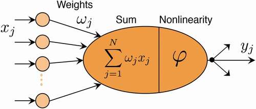
Table 1. Efficiency and speed of various index modulation techniques on silicon photonics. Options for phase modulation of silicon waveguides. a) thermal tuning with TiN filament; b) thermal tuning with embedded photoconductive heater; c) PN/PIN junction across the waveguide for injection and/or depletion modulation; d) III–V/Si hybrid waveguide; e) metal-oxide-semiconductor (MOS), where the ‘metal’ is actually an active semiconductor; f) lithium niobate cladding adds a strong electrooptic effect; g) 2 single-layer-graphene (SLG) ‘capacitor’; h) non-volatile phase change material. This bandwidth was not yet shown experimentally. A big challenge is to reduce the contact resistance with Graphene, reducing RC-loading effect.
Not experimentally shown at high-speed.
Demonstrated up to 20 MHz
Figure 2. Generic system schematic of an analog photonic neural network or photonic tensor core accelerator. The digital-to-analog domain crossings are power costly and ideally a photonic DAC without leaving the optical domain, e.g. Ref [Citation112] would be used instead, thus reducing system complexity and hence allowing for extended scaling laws. The optical processor itself can perform different operations depending on the desired application; is the processor a tensor core accelerator, then it will perform MAC operations such as used directly in VMMs or convolutions, e.g. Ref. Citation138. Is the processor a neural network, then nonlinearity and summations are needed in addition to linear operations. For higher biological plausibility such as for temporal processing of signals at each node, then mapping of partial differential equations onto photonic hardware is needed. This includes spiking neuron approaches where event-driven scheme play a role) [Citation72,Citation85,Citation113–116]
![Figure 2. Generic system schematic of an analog photonic neural network or photonic tensor core accelerator. The digital-to-analog domain crossings are power costly and ideally a photonic DAC without leaving the optical domain, e.g. Ref [Citation112] would be used instead, thus reducing system complexity and hence allowing for extended scaling laws. The optical processor itself can perform different operations depending on the desired application; is the processor a tensor core accelerator, then it will perform MAC operations such as used directly in VMMs or convolutions, e.g. Ref. Citation138. Is the processor a neural network, then nonlinearity and summations are needed in addition to linear operations. For higher biological plausibility such as for temporal processing of signals at each node, then mapping of partial differential equations onto photonic hardware is needed. This includes spiking neuron approaches where event-driven scheme play a role) [Citation72,Citation85,Citation113–116]](/cms/asset/99cdce80-5f68-47a8-aacc-6e9eade34963/tapx_a_1981155_f0002_oc.jpg)
Figure 3. Schematic illustration of photonic neural networks training through in situ backpropagation. Colored squares represent phase shifters. (a) Forward propagation: send in and record the intensity of the electric field
at each phase shifter. (b) Backpropagation: send in error signal
and record the electric field intensity
at each phase shifter and the complex conjugate output
. (c) Interference measurement: send in
to get gradient of the loss function
for all phase shifters simultaneously by extracting
. (Tyler et al., 2018) Hughes et al. (2018)
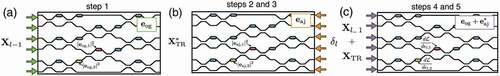
Figure 4. (a) Illustration of pre-synaptic and post-synaptic spikes from two neurons N1 and N2. (b) Illustration of a STDP response. Right purple region: long-term potentiation; Left brown region: long-term depression. tpost-tpre: time difference between the firing of the post- and pre-synaptic spikes. (c) Experimentally measured STDP curves from the photonic based STDP circuit
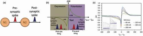
Figure 5. (left) Concept of training and implementing photonic neural networks. Inset shows the NLAF of the photonic neural network measured with real-time signals. The NLAF is realized by a fast O/E/O neuron using a SiGe photodetector connected to a microring modulator with a reverse-biased PN junction embedded in the microring. (right) Constellations of X-polarization of a 32 Gbaud PM-16QAM, with the ANN-NLC gain of 0.57 dB in Q-factor and with the PNN-NLC gain of 0.51 dB in Q-factor [Citation22]
![Figure 5. (left) Concept of training and implementing photonic neural networks. Inset shows the NLAF of the photonic neural network measured with real-time signals. The NLAF is realized by a fast O/E/O neuron using a SiGe photodetector connected to a microring modulator with a reverse-biased PN junction embedded in the microring. (right) Constellations of X-polarization of a 32 Gbaud PM-16QAM, with the ANN-NLC gain of 0.57 dB in Q-factor and with the PNN-NLC gain of 0.51 dB in Q-factor [Citation22]](/cms/asset/e32586e0-4b5e-48c1-912a-4dcaca2d9ece/tapx_a_1981155_f0005_oc.jpg)
Figure 6. (a) Generic model of a reservoir computer [b) Illustration of the RC equalization scheme in Citation162,based on a single nonlinear node with time delayed feedback. The input is a vector of N samples representing a single bit or symbol. The mask vector
, which defines the input weights, is multiplied by the elements in
and injected sequentially into the reservoir. The output is a linear combination of the virtual nodes in the reservoir with weights optimized to produce an estimate
of the bit or symbol value
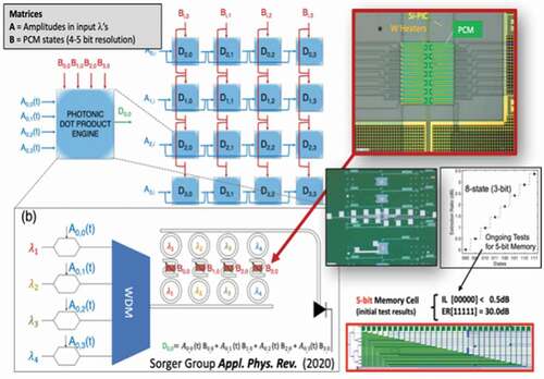
Figure 7. (a) Illustration of the JAR design and the four functional units. (b) Spectral waterfall measurement of the photonic JAR in action with sinusoidal reference signal fR and jamming signals fJ = 150 MHz. (i) fJ is approaching fR from the low frequency side and triggers the JAR, (ii) fJ is approaching fR from the low frequency side and triggers the JAR, and then is moved away
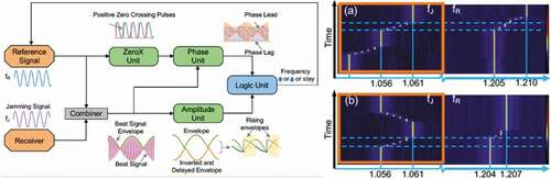
Figure 8. Concept of blind source separation
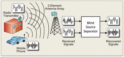
Figure 9. (Comparison of multi-antenna radio front-ends followed by dimensionality reduction. a) Dimensionality reduction with electronic DSP in which each antenna requires an ADC. b) Dimensionality reduction in the analog domain [a.k.a physical layer) in which only one ADC is required. A photonic implementation of weighted addition is pictured, consisting of electrooptic modulation, WDM filtering, and photodetection. From .Citation177
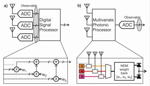
Figure 10. (Experimental waveforms of the received mixtures (left column) and corresponding estimated sources (right column) when performing FastICA (black) and photonic BSS (red) at three frequency bands whose central frequencies are at: (a) 781 MHz, (b) 880 MHz, and [c) 1000 MHz. From .Citation24
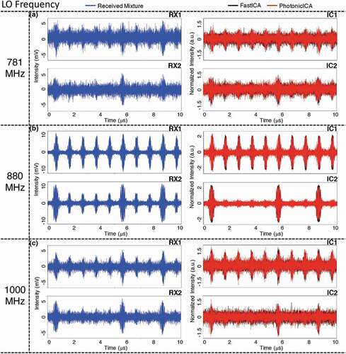
Figure 11. Photonic Tensor Core [PTC) featuring Peta-OPS throughput and 10s ps-short latency to process VMM in PICs Citation138. (left] schematic of a modular exemplary PTC composed of 44 photonic dot-product engines (i.e. 1
4 vector-multiplications) using ring resonators enabling WDM-based parallelism. Data entered via (exemplary) EO modulators at 50 Gbps are MUXed then dropped at passive ring resonators. Being ‘passive’ for the ring resonator is importantly beneficial since it allows for reduced complexity, less real-estate used on the chip, and does not consume power unlike thermally-tuned approaches to perform the optical multiplication. (right) The latter can be elegantly executed using nonvolatile photonic random access memories (P-RAM) based on electrically-programmable phase change materials (PCM). The image shows a prototype of a 3-bit (8-states) binary-written P-RAM element on a Silicon PIC. Using non-GST PCMs enables a rather low (<0.02 dB/state) insertion loss [Citation135]
![Figure 11. Photonic Tensor Core [PTC) featuring Peta-OPS throughput and 10s ps-short latency to process VMM in PICs Citation138. (left] schematic of a modular exemplary PTC composed of 4×4 photonic dot-product engines (i.e. 1×4 vector-multiplications) using ring resonators enabling WDM-based parallelism. Data entered via (exemplary) EO modulators at 50 Gbps are MUXed then dropped at passive ring resonators. Being ‘passive’ for the ring resonator is importantly beneficial since it allows for reduced complexity, less real-estate used on the chip, and does not consume power unlike thermally-tuned approaches to perform the optical multiplication. (right) The latter can be elegantly executed using nonvolatile photonic random access memories (P-RAM) based on electrically-programmable phase change materials (PCM). The image shows a prototype of a 3-bit (8-states) binary-written P-RAM element on a Silicon PIC. Using non-GST PCMs enables a rather low (<0.02 dB/state) insertion loss [Citation135]](/cms/asset/580d3de7-628d-4c9d-9197-a1c5d07e837b/tapx_a_1981155_f0011_oc.jpg)
Figure 12. Example of an Optical Convolutional Neural Network (CNN) accelerator exploiting the massive (106 parallel channel) parallelism of free-space optics. The convolutional filtering is executed as point-wise dot-product multiplication in the Fourier domain. The conversion into and out-of the Fourier domain is performed elegantly and completely passively at zero power While SLM-based systems can perform such Fourier filtering in the frequency domain, the slow update rates does not allow them to outperform GPUs. However, replacing SLMs with fast 10s kHz programmable digital micromirror display [DMD) units, gives such optician CNNs an edge over the top-performing GPUs. Interestingly, the lack-of-phase information of these amplitude-only DMD-based optical CNNs can be accounted for during the NN training process. For details refer to .Citation117
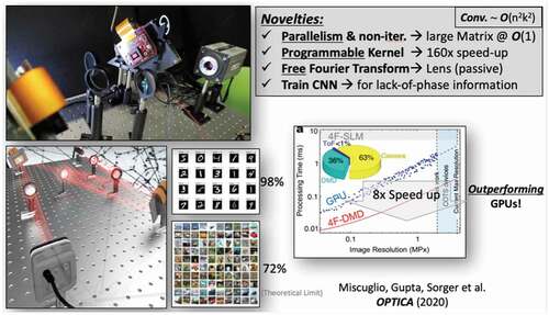
Figure 13. Schematic illustration of a convolution. An input image with dimensionality
(where
,
and
are the height, width and depth of the image, respectively) is convolved with a kernel
with dimensionality
, to produce an image
. Assuming
, the overall output dimensionality is
. The bottom of the figure shows how a convolution operation generalized into a single matrix-matrix multiplication. where the kernel
is transformed into a vector with
elements, and the image is transformed into a matrix of dimensionality
. Therefore, the output is represented by a vector with
elements
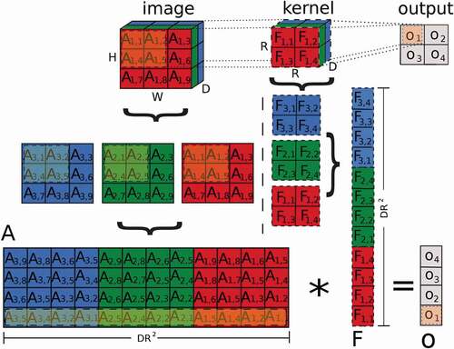
Figure 14. Photonic architecture for producing a single convolved pixel. Input images are encoded in intensities , where the pixel inputs
with
are represented as
,
and
. Considering the boundary parameters, we set
and
. Likewise, the filter values
are represented as are represented as
under the same conditions. We use an array of
lasers with different wavelengths
to feed the MRRs. The input and kernel values,
and
modulate the MRRs via electrical currents proportional to those values. Then, the photonic weight banks will perform the dot products on these modulated signals in parallel. Finally, the voltage adder with resistance
adds all signals from the weight banks, resulting in the convolved feature
![Figure 14. Photonic architecture for producing a single convolved pixel. Input images are encoded in intensities Al,h, where the pixel inputs Am,n,k with m∈[i,i+Rm],n∈[j,j+Rm],k∈[1,Dm] are represented as Al,h, l=1,…,D and h=1,…,R2. Considering the boundary parameters, we set D=Dm and R=Rm. Likewise, the filter values Fm,n,k are represented as are represented as Fl,h under the same conditions. We use an array of R2 lasers with different wavelengths λh to feed the MRRs. The input and kernel values, WCIM_A_1985028 and Fl,h modulate the MRRs via electrical currents proportional to those values. Then, the photonic weight banks will perform the dot products on these modulated signals in parallel. Finally, the voltage adder with resistance R adds all signals from the weight banks, resulting in the convolved feature](/cms/asset/700613ef-04a8-4c47-92cd-06ca4c4a5b77/tapx_a_1981155_f0014_oc.jpg)
Figure 15. Fully parallel and passive convolutions integrated in 3D. (a) 9 convolutional Haar filters and their 3D integration topology using photonic waveguides. (b) SEM micrograph of the 3D printed convolutional filter unit, fabricated with direct laser writing. (c) The filter’s optical transfer function agrees well with the target defined in [a). Figure reproduced from .Citation186
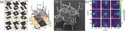
Figure 16. (a] Illustration of a recurrent neural network at time step . (b) Illustration of the recurrent representation of the physical wave system. [c) A vowel classification task on an optical analog recurrent neural network.
is the waveform input signal at the source location.
is the output signal at different probe locations. Figure reproduced from .Citation189
![Figure 16. (a] Illustration of a recurrent neural network at time step t. (b) Illustration of the recurrent representation of the physical wave system. [c) A vowel classification task on an optical analog recurrent neural network. x(t) is the waveform input signal at the source location. Px(t) is the output signal at different probe locations. Figure reproduced from .Citation189](/cms/asset/371fc339-f0e4-4882-b600-e39b43d3548b/tapx_a_1981155_f0016_oc.jpg)
Figure 17. Schematic figure of the procedure to implement the MPC algorithm on a neuromorphic photonic processor. Firstly, map the MPC problem to QP. Then, construct a QP solver with continuous-time recurrent neural networks (CT-RNN) [Citation194]. Finally, build a neuromorphic photonic processor to implement the CT-RNN. The details of how to map MPC to QP, and how to construct a QP solver with CT-RNN are given in De Lima et al. (2019). Adapted from De Lima et al. [Citation27]
![Figure 17. Schematic figure of the procedure to implement the MPC algorithm on a neuromorphic photonic processor. Firstly, map the MPC problem to QP. Then, construct a QP solver with continuous-time recurrent neural networks (CT-RNN) [Citation194]. Finally, build a neuromorphic photonic processor to implement the CT-RNN. The details of how to map MPC to QP, and how to construct a QP solver with CT-RNN are given in De Lima et al. (2019). Adapted from De Lima et al. [Citation27]](/cms/asset/6cbfe70e-f110-4b71-87c7-7c48fc373efa/tapx_a_1981155_f0017_oc.jpg)
Figure 18. Photonic neural network benchmarking against a CPU. (a,b) Phase diagrams of the Lorenz attractor simulated by a conventional CPU (a) and a photonic neural network (b). (c,d) Time traces of simulation variables (blue, green, red) for a conventional CPU (c) and a photonic CTRNN [d). The horizontal axes are labeled in physical real time, and cover equal intervals of virtual simulation time, as benchmarked by CPU and
Pho. The ratio of real-time values of
‘s indicates a 294-fold acceleration. From .Citation118
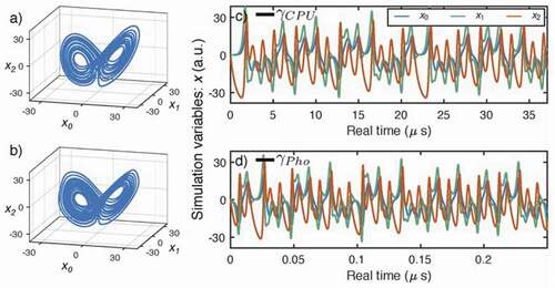
Figure 19. A) Side view (i) no camouflage – fish is visible (ii) silvering – fish is destructively interfered at colors that could indicate the presence of the fish; (b) Bottom view (i) no camouflage – fish appears darker against the bright water surface when seen from below (ii) counterillumination – fish illuminates itself to the same color and intensity as the background. (c) Silvering (i) photonic RF FIR creates destructive interference condition at the stealth signal frequency (fs); (ii) Transmission in optical fiber will only push the constructive interference condition to a much higher frequency (fc+); (iii) Dispersion compensation fiber at the last section of the transmission will move the constructive interference condition back to fc; (iv) Correct dispersion at the stealth receiver allows constructive interference condition to occur at the stealth signal frequency fs. (d) Measured RF spectra and constellation diagrams (i) during transmission without a correct stealth receiver (ii) at the designated stealth receiver with correct location and dispersion
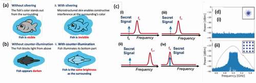
Figure 20. (left) Photonic machine-learning accelerators such as photonic tensor unit (PTU) [.Citation138] enabled a higher level of data security with reduced overhead (e.g. time and power consumption). This opens possibilities for not only securing ‘secure’ and ‘confidential’ data, but also meta-data. [right) Flow-chart for detection of anomalies and misuses exploiting rapidly updating photonic neural network and trained photonic neural network includes programmable nonvolatile photonic memory on-chip for zero-static power consumption processing, once the kernel is written Citation138
![Figure 20. (left) Photonic machine-learning accelerators such as photonic tensor unit (PTU) [.Citation138] enabled a higher level of data security with reduced overhead (e.g. time and power consumption). This opens possibilities for not only securing ‘secure’ and ‘confidential’ data, but also meta-data. [right) Flow-chart for detection of anomalies and misuses exploiting rapidly updating photonic neural network and trained photonic neural network includes programmable nonvolatile photonic memory on-chip for zero-static power consumption processing, once the kernel is written Citation138](/cms/asset/1a46fbcc-bacb-4c42-bfad-b302109b8c28/tapx_a_1981155_f0020_oc.jpg)
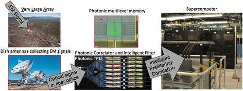
Figure 21. Photonic tensor core and neural networks enable intelligent prefiltering and correlation for scientific discovery, such as between electromagnetic signals collected by Very-Large-Array telescope systems performing intelligent pre-filtering, thus reducing computation load in supercomputers