
Figures & data
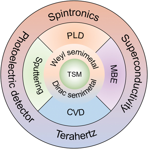
Figure 1. Schematic illustration of the band structures and crystal structures of topological Dirac semimetals and topological Weyl semimetals. (a). The splitting of a Dirac point (DP) into a pair of Weyl points with opposite chirality (WP±) through time-reversal symmetry (TRS) or inversion symmetry (IS) breaking. The green line represents a surface Fermi arc (SFA) between the Weyl points reproduced from reference. Reproduced from [Citation130]. (b). Type-II Weyl semimetal and type-II Dirac semimetal with tilted Weyl or Dirac cones. Reproduced from [Citation130]. (c). Crystal structures of layered topological materials. Blue and purple spheres represent metal and chalcogenide atoms, respectively.
![Figure 1. Schematic illustration of the band structures and crystal structures of topological Dirac semimetals and topological Weyl semimetals. (a). The splitting of a Dirac point (DP) into a pair of Weyl points with opposite chirality (WP±) through time-reversal symmetry (TRS) or inversion symmetry (IS) breaking. The green line represents a surface Fermi arc (SFA) between the Weyl points reproduced from reference. Reproduced from [Citation130]. (b). Type-II Weyl semimetal and type-II Dirac semimetal with tilted Weyl or Dirac cones. Reproduced from [Citation130]. (c). Crystal structures of layered topological materials. Blue and purple spheres represent metal and chalcogenide atoms, respectively.](/cms/asset/29093723-d7a5-4cc1-9715-0369dc278578/tapx_a_2034529_f0001_oc.jpg)
Figure 2. CVD growth of MoTe2 and PtTe2 by tellurizing corresponding metal films. (a). Top is a two-zone furnace growth schematic. Middle and bottom are TEM cross-section images of a 14-cycle MoOx film and converted MoTe2 film, respectively. Reproduced from [Citation62]. (b). Schematic of the CVD process with a half-open quartz tube. Reproduced from [Citation67]. (c). The photograph of wafer-scale PtTe2 films with different thicknesses of ≈ 5 nm (top) and ≈ 10 nm (bottom). Reproduced from [Citation67]. (d). Photo image of PtTe2 films on different substrates. Reproduced from [Citation68].
![Figure 2. CVD growth of MoTe2 and PtTe2 by tellurizing corresponding metal films. (a). Top is a two-zone furnace growth schematic. Middle and bottom are TEM cross-section images of a 14-cycle MoOx film and converted MoTe2 film, respectively. Reproduced from [Citation62]. (b). Schematic of the CVD process with a half-open quartz tube. Reproduced from [Citation67]. (c). The photograph of wafer-scale PtTe2 films with different thicknesses of ≈ 5 nm (top) and ≈ 10 nm (bottom). Reproduced from [Citation67]. (d). Photo image of PtTe2 films on different substrates. Reproduced from [Citation68].](/cms/asset/49a015ad-16a2-4165-8bee-ed6242dd1093/tapx_a_2034529_f0002_oc.jpg)
Figure 3. MBE growth of MoTe2 and WTe2 films. (a). Schematic diagram of the MBE growth setup for MoTe2. Reproduced from [Citation76]. (b). Growth process control of the MBE growth of 1T’ and 2H MoTe2. Reproduced from [Citation76]. (c). Raman spectra of the MoTe2 films grown at different temperatures. Reproduced from [Citation76]. (d). RHEED patterns of graphene substrate (top) and sub-monolayer 1T’ WTe2 (bottom). Reproduced from [Citation50]. (e). Core level spectra of 1T’ WTe2. Reproduced from [Citation50]. (f). Atomically resolved STM image of 1T’ WTe2. Reproduced from [Citation50].
![Figure 3. MBE growth of MoTe2 and WTe2 films. (a). Schematic diagram of the MBE growth setup for MoTe2. Reproduced from [Citation76]. (b). Growth process control of the MBE growth of 1T’ and 2H MoTe2. Reproduced from [Citation76]. (c). Raman spectra of the MoTe2 films grown at different temperatures. Reproduced from [Citation76]. (d). RHEED patterns of graphene substrate (top) and sub-monolayer 1T’ WTe2 (bottom). Reproduced from [Citation50]. (e). Core level spectra of 1T’ WTe2. Reproduced from [Citation50]. (f). Atomically resolved STM image of 1T’ WTe2. Reproduced from [Citation50].](/cms/asset/971a0d37-daa8-4ea2-a8da-e9d75b87656d/tapx_a_2034529_f0003_oc.jpg)
Figure 4. Preparation and characterization of PLD growth of WTe2 films. (a). Schematic diagrams of the PLD and post annealing apparatus for WTe2 films. Reproduced from [Citation94]. (b). Raman spectra of the WTe2 films annealed for different time intervals. Reproduced from [Citation94]. (c). Cross-section HAADF image of a multilayered Bi2Te3-WTe2 film grown on mica. Reproduced from [Citation96]. (d). Higher magnification scan of the boxed area shown in Figure 4(c). Reproduced from [Citation96].
![Figure 4. Preparation and characterization of PLD growth of WTe2 films. (a). Schematic diagrams of the PLD and post annealing apparatus for WTe2 films. Reproduced from [Citation94]. (b). Raman spectra of the WTe2 films annealed for different time intervals. Reproduced from [Citation94]. (c). Cross-section HAADF image of a multilayered Bi2Te3-WTe2 film grown on mica. Reproduced from [Citation96]. (d). Higher magnification scan of the boxed area shown in Figure 4(c). Reproduced from [Citation96].](/cms/asset/736ff4f0-44e1-4afe-8f8a-aab7bc883563/tapx_a_2034529_f0004_oc.jpg)
Figure 5. (a). Schematic illustration of the post annealing SiO2/MoTe2/SiO2 heterostructure. Reproduced from [Citation102]. (b). Schematic diagram of the co-sputtering deposition of MoTe2. Reproduced from [Citation54]. (c). Plot of deposition rate and the Te/Mo ratio (inset) vs. temperature. Reproduced from [Citation54]. (d). Schematic illustration of the transformation of the as-deposited MoTe2 films. Reproduced from [Citation103].
![Figure 5. (a). Schematic illustration of the post annealing SiO2/MoTe2/SiO2 heterostructure. Reproduced from [Citation102]. (b). Schematic diagram of the co-sputtering deposition of MoTe2. Reproduced from [Citation54]. (c). Plot of deposition rate and the Te/Mo ratio (inset) vs. temperature. Reproduced from [Citation54]. (d). Schematic illustration of the transformation of the as-deposited MoTe2 films. Reproduced from [Citation103].](/cms/asset/ece9e60b-b969-4e47-8245-f6d444a11230/tapx_a_2034529_f0005_oc.jpg)
Table 1. List of large-area growth conditions for 2D layered topological semimetals
Figure 6. The transport characteristics of the MBE growth PdTe2 films. (a). The resistance of PdTe2 films with different thickness as a function of the temperature. The inset is the schematic of four-probe measurements. Reproduced from [Citation112]. (b). Tc and Hc2 (T = 0) dependence of the film thickness. The circles and squares represent the Hc2 (0) derived from the two-band model and Ginzburg-Landau formula, respectively. Reproduced from [Citation112]. (c). The sheet resistance Rs of PdTe2 films under the conditions of different perpendicular magnetic fields from 0 to 0.897 T. Reproduced from [Citation113]. (d). The evolution of Rs-B curves at different temperatures ranging from 20 to 450 mK. The inset curves are some crossing points from the Rs-B. Reproduced from [Citation74].
![Figure 6. The transport characteristics of the MBE growth PdTe2 films. (a). The resistance of PdTe2 films with different thickness as a function of the temperature. The inset is the schematic of four-probe measurements. Reproduced from [Citation112]. (b). Tc and Hc2 (T = 0) dependence of the film thickness. The circles and squares represent the Hc2 (0) derived from the two-band model and Ginzburg-Landau formula, respectively. Reproduced from [Citation112]. (c). The sheet resistance Rs of PdTe2 films under the conditions of different perpendicular magnetic fields from 0 to 0.897 T. Reproduced from [Citation113]. (d). The evolution of Rs-B curves at different temperatures ranging from 20 to 450 mK. The inset curves are some crossing points from the Rs-B. Reproduced from [Citation74].](/cms/asset/558c0676-74fc-469d-b860-d3dc27de549a/tapx_a_2034529_f0006_oc.jpg)
Figure 7. Photoelectric detection researches of PtTe2 films. (a). The photoresponse of PtTe2 at different wavelengths. The inset is the schematic illustration of photodetector. Reproduced from [Citation72]. (b). Anisotropic photoresponse for the linear-polarized excitation at 10.7 μm. Reproduced from [Citation72]. (c). The schematic illustration of the temporal photo-responsiveness of PtTe2/p-Si devices. Reproduced from [Citation49]. (d). Relative balance as a function of illumination modulation frequency, defined as (Imax− Imin)/Imax. Reproduced from [Citation49]. (e). The rise (τr) and fall (τf) times are obtained in the magnified view of photo-switching characteristics at 150 kHz. Reproduced from [Citation49]. (f). Photographs and images of the PtTe2-based arrays device. Reproduced from [Citation118]. (g), (h). The THz detecting devices and mechanisms of PtTe2 and graphene heterojunction, respectively. Reproduced from [Citation121]. (i). THz image of the metal nut. Reproduced from [Citation121].
![Figure 7. Photoelectric detection researches of PtTe2 films. (a). The photoresponse of PtTe2 at different wavelengths. The inset is the schematic illustration of photodetector. Reproduced from [Citation72]. (b). Anisotropic photoresponse for the linear-polarized excitation at 10.7 μm. Reproduced from [Citation72]. (c). The schematic illustration of the temporal photo-responsiveness of PtTe2/p-Si devices. Reproduced from [Citation49]. (d). Relative balance as a function of illumination modulation frequency, defined as (Imax− Imin)/Imax. Reproduced from [Citation49]. (e). The rise (τr) and fall (τf) times are obtained in the magnified view of photo-switching characteristics at 150 kHz. Reproduced from [Citation49]. (f). Photographs and images of the PtTe2-based arrays device. Reproduced from [Citation118]. (g), (h). The THz detecting devices and mechanisms of PtTe2 and graphene heterojunction, respectively. Reproduced from [Citation121]. (i). THz image of the metal nut. Reproduced from [Citation121].](/cms/asset/e71f9b1b-810f-41e2-9303-797a3f673b10/tapx_a_2034529_f0007_oc.jpg)
Figure 8. The spin orbit torque measurements in the WSMs and DSMs. (a). Illustration of the second harmonic measurement on WTex(3, 5, 8 nm)/CoFeB(6 nm) Hall bar device. Reproduced from [Citation100]. (b). The thickness dependent DL torque and FL torque of the sample in Figure 8(a). Reproduced from [Citation100]. (c). The DL torque efficiency of different thickness and Te concentration in WTex films. Reproduced from [Citation101]. (d), (e). The schematic illustration and image of the Py/WTe2 devices. Reproduced from [Citation125]. (f). MOKE images of Py before (left) and after (right) applying a pulsed DC current I (indicated by the purple arrow) along the x-axis. Reproduced from [Citation125]. (g). The schematic illustration of the torque generation in the Py/PtTe2 heterojunction. Reproduced from [Citation67]. (h). The inverse of the SOT efficiency as an evolution of the inverse of the Py thickness in Pt/Py and PtTe2/Py. Reproduced from [Citation67]. (i). ξSOT (circle line) and spin Hall conductivity (circle) with different PtTe2 thicknesses. Reproduced from [Citation67].
![Figure 8. The spin orbit torque measurements in the WSMs and DSMs. (a). Illustration of the second harmonic measurement on WTex(3, 5, 8 nm)/CoFeB(6 nm) Hall bar device. Reproduced from [Citation100]. (b). The thickness dependent DL torque and FL torque of the sample in Figure 8(a). Reproduced from [Citation100]. (c). The DL torque efficiency of different thickness and Te concentration in WTex films. Reproduced from [Citation101]. (d), (e). The schematic illustration and image of the Py/WTe2 devices. Reproduced from [Citation125]. (f). MOKE images of Py before (left) and after (right) applying a pulsed DC current I (indicated by the purple arrow) along the x-axis. Reproduced from [Citation125]. (g). The schematic illustration of the torque generation in the Py/PtTe2 heterojunction. Reproduced from [Citation67]. (h). The inverse of the SOT efficiency as an evolution of the inverse of the Py thickness in Pt/Py and PtTe2/Py. Reproduced from [Citation67]. (i). ξSOT (circle line) and spin Hall conductivity (circle) with different PtTe2 thicknesses. Reproduced from [Citation67].](/cms/asset/da4c503f-5ac6-4312-b7e2-412efe6a90c7/tapx_a_2034529_f0008_oc.jpg)