
Figures & data

Figure 1. (a) Sketch of the band structure of the nodal-line semimetal and the drumhead-like surface states in the surface Brillouin zone. (b) Torus-shaped Fermi surface.
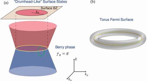
Figure 2. (a) Torus-shaped Fermi surface, with major radius , minor radius
, toroidal angle
, and poloidal angle
. (b) The impurity potentials results in 3D and 2D diffusion behaviors, respectively. (c) A coherent backscattering process from wave vector
to
around the toroidal direction, which is a 3D diffusion behavior. (d) Backscattering from wave vector
to
around poloidal direction, which is a 2D diffusion behavior [Citation54].
![Figure 2. (a) Torus-shaped Fermi surface, with major radius k0, minor radius κ, toroidal angle θ, and poloidal angle φ. (b) The impurity potentials results in 3D and 2D diffusion behaviors, respectively. (c) A coherent backscattering process from wave vector k to −k around the toroidal direction, which is a 3D diffusion behavior. (d) Backscattering from wave vector δk to −δk around poloidal direction, which is a 2D diffusion behavior [Citation54].](/cms/asset/698a52ee-2f05-4685-aff3-f0d814ae9b9c/tapx_a_2065216_f0002_oc.jpg)
Figure 3. Relevant Feynman diagrams. (a) Three leading-order diagrams of the quantum interference corrections to the conductivity, with one bare Hikami box and two dressed Hikami boxes. The arrowed solid line represents Green functions and the arrowed dashed line represents impurity scattering. (b) Ladder diagram vertex correction to the velocity. (c) The Cooperon correction [Citation54].
![Figure 3. Relevant Feynman diagrams. (a) Three leading-order diagrams of the quantum interference corrections to the conductivity, with one bare Hikami box and two dressed Hikami boxes. The arrowed solid line represents Green functions and the arrowed dashed line represents impurity scattering. (b) Ladder diagram vertex correction to the velocity. (c) The Cooperon correction [Citation54].](/cms/asset/de33b74e-2f3b-4910-9f99-251cf192dab5/tapx_a_2065216_f0003_oc.jpg)
Figure 4. The magnetoconductivity in the (a) SR limit and (b) LR limit for different phase coherence lengths
, which are represent by the different color [Citation54].
![Figure 4. The magnetoconductivity δσz(B) in the (a) SR limit and (b) LR limit for different phase coherence lengths ℓϕ, which are represent by the different color [Citation54].](/cms/asset/1ffc2935-3452-43c7-879b-13532fa9a49b/tapx_a_2065216_f0004_oc.jpg)
Figure 5. (a) The maximum () and minumum (
) cross sections in the nodal-line plane of the torus Fermi surface. (b) The maximum (
) and minimum (
) cross sections out of the nodal-line plane of the torus Fermi surface [Citation66].
![Figure 5. (a) The maximum (α) and minumum (β) cross sections in the nodal-line plane of the torus Fermi surface. (b) The maximum (γ) and minimum (δ) cross sections out of the nodal-line plane of the torus Fermi surface [Citation66].](/cms/asset/74deefdd-bf80-414b-94f8-aa09a20a480d/tapx_a_2065216_f0005_oc.jpg)
Table 1. The phase shift of nodal-line semimetals in [Citation66]
Figure 6. (a) Schematic diagram of the torus-shaped Fermi surface in nodal-line semimetal, the major radius is , minor radius is
, the toroidal angle and poloidal angle are
,
, respectively. (b) Finite berry curvature distribution in the poloidal cross section. (c-e) The deformation process of the Fermi surface induced by the increasing external magnetic field [Citation97].
![Figure 6. (a) Schematic diagram of the torus-shaped Fermi surface in nodal-line semimetal, the major radius is k0, minor radius is κ, the toroidal angle and poloidal angle are θ,ϕ, respectively. (b) Finite berry curvature distribution in the poloidal cross section. (c-e) The deformation process of the Fermi surface induced by the increasing external magnetic field [Citation97].](/cms/asset/02bb3743-f9ce-4fae-9bf3-113583763216/tapx_a_2065216_f0006_oc.jpg)
Figure 7. (a) MR as a function of the external magnetic field with and without sign reversal. (b) Correspondence between MR’s sign reversal point and the critical magnetic field (open circles) [Citation97].
![Figure 7. (a) MR as a function of the external magnetic field with and without sign reversal. (b) Correspondence between MR’s sign reversal point and the critical magnetic field B∗ (open circles) [Citation97].](/cms/asset/9ec77d10-030f-4bb6-ae65-ed7d2facbb87/tapx_a_2065216_f0007_oc.jpg)
Figure 8. Three types of AR, (a) RAR, (b) SAR, (d) AAR. (c) torus-shaped Fermi surface [Citation101].
![Figure 8. Three types of AR, (a) RAR, (b) SAR, (d) AAR. (c) torus-shaped Fermi surface [Citation101].](/cms/asset/24ac82dd-7174-4e56-a7f5-a9c0b3d249ef/tapx_a_2065216_f0008_oc.jpg)
Table 2. Different features in the RAR, SAR, and AAR [Citation101]
Figure 9. (a)The two-terminal setup for detecting the AAR. (b) Nonlocal conductance in RAR regime. (c) (d) Nonlocal conductance in AAR regime with different interface barrier [Citation101].
![Figure 9. (a)The two-terminal setup for detecting the AAR. (b) Nonlocal conductance in RAR regime. (c) (d) Nonlocal conductance in AAR regime with different interface barrier [Citation101].](/cms/asset/3bc4d59b-b9d7-4623-a2cf-62608630e072/tapx_a_2065216_f0009_oc.jpg)
Figure 10. (a) A junction between normal metal and nodal-line semimetal, The drumhead-like surface state at the boundary are encircled by the projection of the bulk nodal loop onto the surface Brillouin zone. The inset show trivial (dashed line) and nontrivial (solid line) band dispersion. (b) Probability of spin-flipped reflection [Citation101].
![Figure 10. (a) A junction between normal metal and nodal-line semimetal, The drumhead-like surface state at the boundary are encircled by the projection of the bulk nodal loop onto the surface Brillouin zone. The inset show trivial (dashed line) and nontrivial (solid line) band dispersion. (b) Probability of spin-flipped reflection [Citation101].](/cms/asset/c12a0174-66aa-498d-9f0b-d0736fa2fd41/tapx_a_2065216_f0010_oc.jpg)
Figure 11. (a) Setup for detecting DSS with spin transport. (b) The spin (thick lines) and charge (thin lines) with different interface barrier heights. (c) Effect of finite dispersion of DSS on the spin conductance, where the interface barrier . (d) Setup for detecting DSS with charge transport. (e) Charge conductance with different interface barrier heights. (f) Effect of finite dispersion of DSS on the charge conductance, where the interface barrier
[Citation105].
![Figure 11. (a) Setup for detecting DSS with spin transport. (b) The spin (thick lines) and charge (thin lines) with different interface barrier heights. (c) Effect of finite dispersion of DSS on the spin conductance, where the interface barrier Z=10. (d) Setup for detecting DSS with charge transport. (e) Charge conductance with different interface barrier heights. (f) Effect of finite dispersion of DSS on the charge conductance, where the interface barrier Z=10 [Citation105].](/cms/asset/138b7119-a716-4f9f-b11d-ed53b394d8f5/tapx_a_2065216_f0011_oc.jpg)
Figure 12. MR measurements of ZrSiS. (a) The curves of MR in different temperatures. (b) The MR curves with different measurement angles. (c) The MR data in the log-log frame. (d) The MR’s angular dependence, forming a butterfly shape [Citation87].
![Figure 12. MR measurements of ZrSiS. (a) The curves of MR in different temperatures. (b) The MR curves with different measurement angles. (c) The MR data in the log-log frame. (d) The MR’s angular dependence, forming a butterfly shape [Citation87].](/cms/asset/735f2875-da42-4343-8582-84a990eadd0c/tapx_a_2065216_f0012_oc.jpg)