
Figures & data
Table 1. Physical properties of SQW and BL used in the work. is the mass of an electron and
is the vacuum permittivity.
Figure 1. (a) Cross section of the GaAsBi/AlGaAs SQW structure under investigation. (b) Schematic band diagram of modulation-doped quantum well structure GaAs1-yBiy separated by an AlxGa1−xAs as barrier layer (BL).
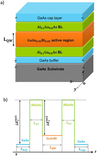
Table 2. Summary of the used abbreviations.
Figure 2. The conduction band profiles for the studied structures A (a), B (b), and (c) along the - direction. The left contact on the CB was set to zero energy arbitrarily.
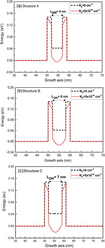
Figure 3. Energy level diagram of GaAsBi/AlGaAs SQW for the three studied structures A, B, and C. ISBT for structure a is ISBT1A, for structure B are respectively ISBT1B, ISBT2B, and for structure C are respectively ISBT1C, ISBT2C, SBT3C.
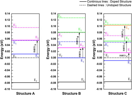
Figure 4. The 3D electron density for structures A (a), B (b), and (c).
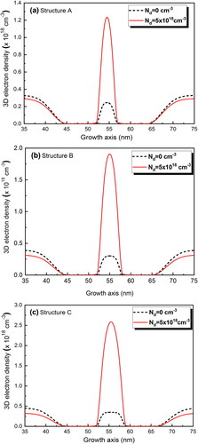
Figure 5. The absorption coefficient AC for structures A (a), B (b), and C (c) for doped and undoped GaAsBi/AlGaAs heterostructures.
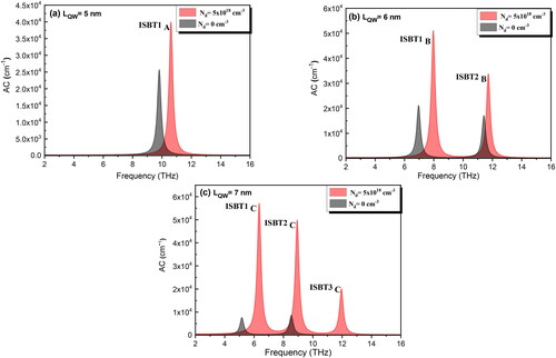
Figure 6. The variation in the intensity difference of the absorption coefficient, between doped and undoped structures for the GaAsBi active layer thickness.
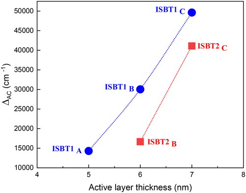
Figure 7. (a) 3D plot showing the variation of the absorption coefficient (AC) with frequency and active layer thickness at a fixed doping concentration (). (b) 3D plot depicting the variation of the AC with frequency and active layer doping concentration at a fixed quantum well width (
).
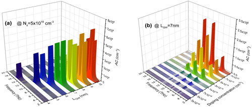
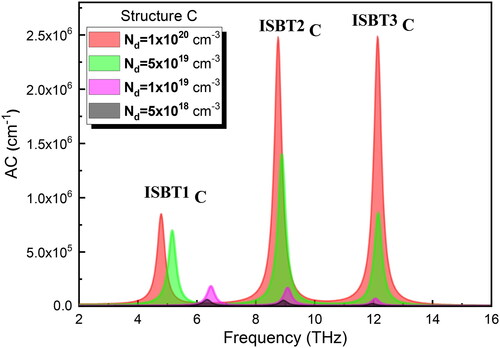
Figure 8. Structure C absorption coefficient at different doping levels of GaAsBi quantum well.
Data availability
All results exist in the main manuscript.