Figures & data
Figure 1. (a) SEM image of mixed CoCrFeNiCu powders; (b) SEM image of mixed Al0.8CoCrFeNiCu powders.
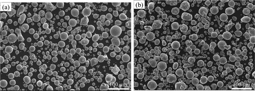
Table 1. Processing parameters for fabricating the HEA blocks in this study.
Figure 2. SEM images of microstructures of CoCrCuFeNi HEAs with different VEDs: (a) VED = 60 J/mm3; (b) VED = 80 J/mm3; (c) VED = 120 J/mm3; (d) VED = 160 J/mm3.
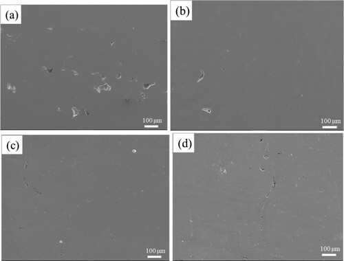
Figure 3. The EDS map scanning results of CoCrCuFeNi HEAs around the pore (60 J/mm3).
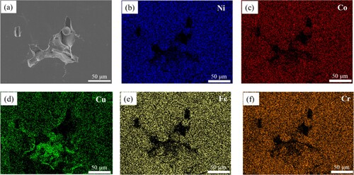
Figure 4. The EDS map scanning results of CoCrCuFeNi HEAs at crack (160 J/mm3).
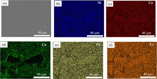
Figure 5. The EDS map scanning results of CoCrCuFeNi HEAs in the crack-free area (80 J/mm3).
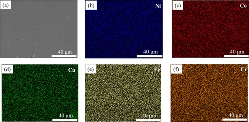
Figure 6. EBSD images of CoCrCuFeNi HEAs with different VEDs: (a) VED = 60 J/mm3; (b) VED = 80 J/mm3; (c) VED = 120 J/mm3; (d) VED = 160 J/mm3.
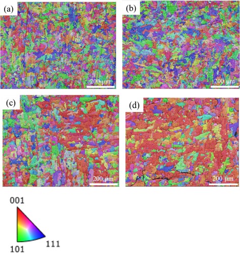
Figure 7. Distribution of grain boundaries of CoCrCuFeNi HEAs with different VEDs: (a) VED = 60 J/mm3; (b) VED = 80 J/mm3; (c) VED = 120 J/mm3; (d) VED = 160 J/mm3.
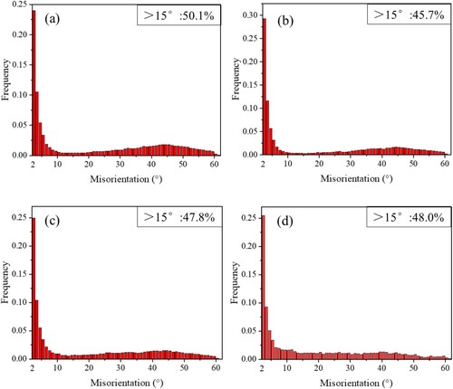
Figure 8. XRD patterns of AlxCoCrCuFeNi (x = 0, 0.8) HEAs with different VEDs.
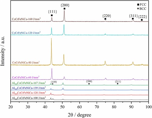
Table 2. Content of each element in Al0.8CoCrCuFeNi HEA samples.
Figure 9. SEM images of the surface of Al0.8CoCrCuFeNi HEAs with different VEDs: (a) VED = 100 J/mm3; (b) VED = 120 J/mm3; (c) VED = 139 J/mm3; (d) VED = 167 J/mm3.
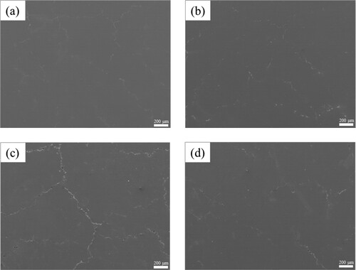
Figure 10. The SEM image and EDS elemental maps showing the liquation cracks of Al0.8CoCrCuFeNi HEA fabricated with 167 J/mm3.
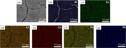
Figure 11. The EBSD images of Al0.8CoCrCuFeNi HEAs with different VEDs: (a) VED = 100 J/mm3; (b) VED = 120 J/mm3; (c) VED = 139 J/mm3; (d) VED = 167 J/mm3.
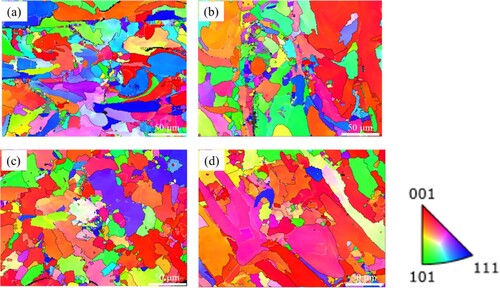
Figure 12. Distribution of FCC phase and BCC phase of Al0.8CoCrCuFeNi HEAs with different VEDs (Green area: FCC phase; Red area: BCC phase); (a) VED = 100 J/mm3; (b) VED = 120 J/mm3; (c) VED = 139 J/mm3; (d) VED = 167 J/mm3.
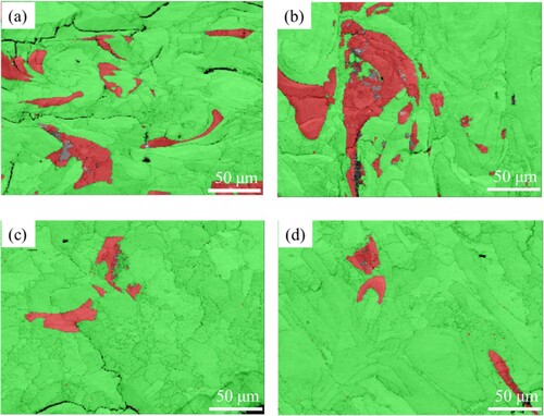
Figure 13. Microhardness of AlxCoCrCuFeNi (x = 0, 0.8) HEAs with different VEDs.
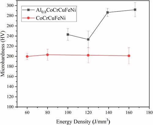
Figure 14. Engineering stress-strain curves of AlxCoCrCuFeNi (x = 0, 0.8) HEAs with different VEDs.
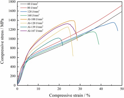
Figure 15. XRD patterns of the as-deposited Al0.8CoCrCuFeNi HEAs after annealing treatment.
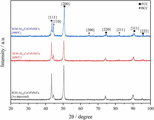
Figure 16. SEM images of the as-deposited Al0.8CoCrCuFeNi HEAs after annealing treatment at different temperatures: (a) 600°C (X-Y plane); (b) 900°C (X-Y plane); (c) 600°C (X-Z plane); (d) 900°C (X-Z plane).
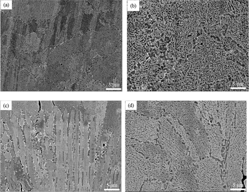
Figure 17. Microhardness of the as-deposited Al0.8CoCrCuFeNi HEAs after annealing treatment.
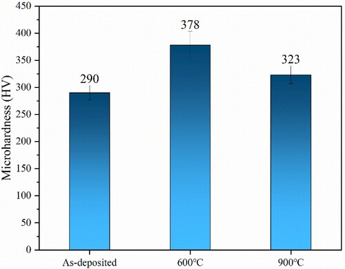
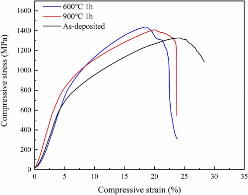
Figure 18. Compressive engineering stress-strain curves of the as-deposited and heat treated Al0.8CoCrCuFeNi HEAs.