Figures & data

Figure 1. Bottom-up material synthesis with NPs and their self-assemblies. (a) Schematics illustrating the formation of a device using top-down and bottom-up self-assembly. (b) Schematic showing the use of NPs for assembly onto a substrate with increasing level of structural control. (c) Schematic illustration of the use of plasmonic substrates as plasmon enhanced fluorescence platforms.
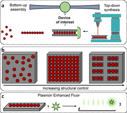
Figure 2. NPs into self-assembled materials. (a) TEM images showing the transformation of a binary NP superlattice composed of gold (Au) and iron oxide (Fe3O4) NPs into non-close packed superlattices by selectively removing/etching one of the two NP components. Inset scale bars are 5 nm (Udayabhaskararao et al., Citation2017). (b) SEM image showing the surface morphology of a NP supercrystal stabilized by H-bonding interactions. Upon sintering into a macroscopic material, exceptional control can be gained over the grain size of the crystallites (c, d). Each crystalline grain is colored differently (Santos et al., Citation2021). (e) SEM images showing the formation of Au nanorod (NR) dimers assembled using pre-defined cavities on a substrate. The SEM images on the right show the deterministic variation of interparticle distance between NR dimers (Flauraud et al., Citation2017).
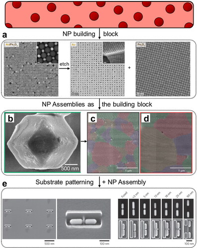
Figure 3. Solution phase growth of AuNPs directly on substrates. (a) Scanning electron microscopy (SEM) image of a solution phase grown plasmonic Au nanoisland film pGold. (b) Schematic illustration of a sandwich immunoassay for detecting myocardial infarction biomarkers (cTnI/CK-MB) on a pGold chip. (c) Calibration curves comparing the fluorescence signal and detection limits for cTnI on pGold (red), glass (blue), and sputtered gold (sGold) (yellow) chips (Xu et al., Citation2020). (d) Schematic of the solution phase growth of AuNPs on glass slides assisted by block copolymer micelle nanolithography (BCMN). (e) SEM images showing the distribution of AuNPs after dip-coating and oxygen plasma for copolymer etching, before solution phase growth; and (f) after the growth process. (g) Schematic showing the interparticle distance in both cases. (h) Immunoassay Ab-PfLDH-aptamer sandwich scheme. The fluorophore is placed at approximately 10 nm from the Au surface, maximizing fluorescence enhancement (Minopoli et al., Citation2022).
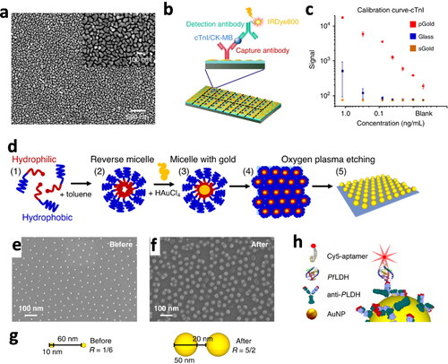
Table 1. Plasmon fluorescence enhancement studies of colloidal AuNPs on planar substrates.
Figure 4. Adsorption of AuNPs onto substrates by electrostatic interactions. (a) Schematic diagram of the adsorption of negatively charged citrate-coated AuNPs on positively charged amino functionalized glass slides, followed by layer-by-layer deposition of positive PHA and negative PSS polyelectrolytes, to form a spacer layer for the dye (Chekini et al., Citation2015). (b) Schematic view of the self-assembly of Au nanorods on a silicon substrate, with a polyelectrolyte spacer and lanthanide-doped upconverting nanoparticles (UCNPs). (c) Scanning electron microscopy images of Au nanorods and (d) UCNPs, on the polyelectrolyte-coated substrate. (e) Correlation of fluorescence intensity (red line) and electric field intensity (black line) with spacer thickness (Feng, You, et al., Citation2015). (f) Schematic view of the fabrication of a flexible polydimethylsiloxane (PDMS) plasmonic patch with electrostatically adsorbed AuNPs and application of standard fluoroimmunoassays. (g) SEM images of Au core/Ag shell cubes and two sizes of Au nanorods absorbed onto the PDMS plasmonic patch (Luan et al., Citation2018).
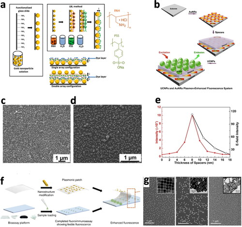
Figure 5. (a) Thiol–Au binding of AuNPs. (a1) Schematic of Au nanostars bound to thiol-modified glass slides. Corresponding (a2) SEM images of adsorbed small (∼50 nm) and (a3) large (215 nm) Au nanostars (insert: TEM of individual nanostars) (Theodorou et al., Citation2019). (b) Spin-coating of AuNPs. (b1) Schematic showing AuNPs functionalized with a dense polystyrene shell, followed by spin-coating onto a substrate and oxygen plasma etching of the polystyrene shell. (b2) SEM images of Au nanospheres and (b3) Au nanorods with shorter (left) and larger (right) polystyrene chains (Ullrich et al., Citation2013). (c) Surface plasmon-coupled emission (SPCE) sensor with spin-coated AuNPs. (c1) Schematic of the SPCE sensing platform. (Bhaskar, Kowshik, et al., Citation2020). (c2) SEM image of heterometallic AgAu nanocubes. (c3) Fluorescent enhancement values obtained for different nanointerface designs (Bhaskar et al., Citation2022). (d) Nanoparticle-on-mirror (NPoM) nanocavities. (d1) Schematic showing the high optical field confinement in the gap (yellow) and (d2) fluorescence emission with and without the Cy5 dye incorporated into the nanocavity. (d3) Purcell enhancement results relative to the position of Cy5 from the center of the gap, experimental emission (orange points) and theoretically calculated emission for vertical (90°) dipole (solid blue) and tilted (45°) dipole (dashed blue). Calculated quantum efficiency for vertical dipole (dashed gray line) (Chikkaraddy et al., Citation2018).
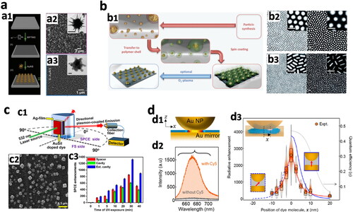
Figure 6. Interfacial assembly of AuNPs. (a) Schematic of the fabrication of plasmonic substrates by interfacial assembly, AuNPs organized into monolayers at the water/chloroform interface are transferred to a glass substrate. (b) Extinction spectra of substrates obtained by assembly of Au@Ag nanocubes, Au@Ag nanorods, and Au nanorods, respectively. (c) SEM of the assembled plasmonic substrates on glass slides (scale bars: 400 nm). (d) Schematic of total internal reflection fluorescence (TIRF) microscopy using interfacially assembled plasmonic substrates with enhanced fluorescence resonance energy transfer (FRET) imaging. (e) Fluorescence images of MDA-MB-468 cells on glass and (f) on a plasmonic substrate (scale bar: 20 µm) (Hou et al., Citation2020).
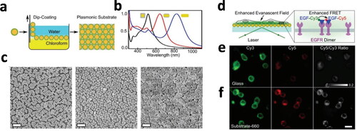
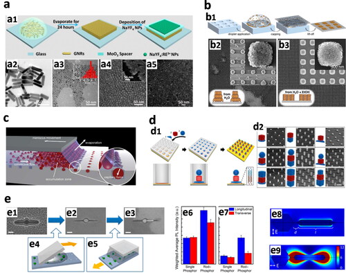
Figure 7. (a) Controlled-evaporation self-assembly. (a1) Schematic of the process: a drop of AuNR dispersion is evaporated under controlled conditions, originating a vertically aligned monolayer of Au nanorods, followed by the deposition of NaYF4:Yb3+, Er3+ upconversion nanoparticles (UCNP), separated by a MoO3 spacer. (a2) TEM images of Au nanorods and (a3) UCNP. (a4) SEM images of vertically aligned Au nanorods (insert, side view) and (a5) random aggregates of Au nanorods (Yin et al., Citation2016). (b) Template-controlled self-assembly. (b1) Schematic depicting a drop of AuNP dispersion confined between the PDMS mold and the substrate; upon drying and PDMS lift-off organized supercrystals are obtained. (b2) SEM images of standing AuNRs obtained when dispersed in water or (b3) laying AuNR supercrystal arrays when dispersed in a water/ethanol mixture (Hanske et al., Citation2019). (c) Schematic of capillary-assisted self-assembly, AuNPs are directed and trapped into template cavities by capillary forces (Ni et al., Citation2018). (d) DNA-assisted self-assembly. (d1) Schematic of polymer PMMA holes and sequential assembly of ssDNA-modified AuNPs with complementary sequences. (d2) SEM images of two- and three-layer stacks of AuNP superlattices (scale bar: 300 nm) (Lin et al., Citation2018). (e) Templated self-assembly of heterodimers composed of UCNP and AuNR on a silicon substrate. SEM images of (e1) empty cavities, (e2) single UCNP, and (e3) heterodimer UCNP/AuNR in SiO2 template (Scale bars: 100 nm). (e4) Schematic of UCNP assembly with ‘squeegee method’ and (e5) AuNRs positioned in the cavities by capillary-assisted assembly. (e6) Inverse-variance weighted average photoluminescence (PL) intensity for a power density of 1.6 × 10⁶ W/cm2 and (e7) 1.6 × 10⁵ W/cm2. (e8) simulated transverse and (e9) longitudinal excitation polarization field intensity enhancement maps (Greybush et al., Citation2014).