
Figures & data
Figure 1. (a) MSM device structure, (b) I-V characteristics of the photoconductor in comparison with a typical MSM-PD during 220 nm light illumination with a light intensity of ∼20 µW/cm2. (c) Normalized spectral photoresponse of the MSM-PD and the photoconductor. (d) Time response of the photoconductor upon the 220 nm light illumination measured by a mechanical chopping method [Citation67]. © 2006, American Institute of Physics.
![Figure 1. (a) MSM device structure, (b) I-V characteristics of the photoconductor in comparison with a typical MSM-PD during 220 nm light illumination with a light intensity of ∼20 µW/cm2. (c) Normalized spectral photoresponse of the MSM-PD and the photoconductor. (d) Time response of the photoconductor upon the 220 nm light illumination measured by a mechanical chopping method [Citation67]. © 2006, American Institute of Physics.](/cms/asset/54ae12a8-3c5c-4ac7-8b29-7798ec440f6f/tfdi_a_1877019_f0001_c.jpg)
Figure 2. (a) Optical image of the diamond SPD, (b) Dark I-V characteristics of the diamond/WC photodiode before and after annealing at 500 °C for 3 h. (c) Reverse I-V characteristics under the 220 nm light illumination before and after annealing at 500 °C for 3 h. (d) Transient response of the diamond/WC photodiode to DUV after annealing for 3 h [Citation70]. © 2005The Japan Society of Applied Physics.
![Figure 2. (a) Optical image of the diamond SPD, (b) Dark I-V characteristics of the diamond/WC photodiode before and after annealing at 500 °C for 3 h. (c) Reverse I-V characteristics under the 220 nm light illumination before and after annealing at 500 °C for 3 h. (d) Transient response of the diamond/WC photodiode to DUV after annealing for 3 h [Citation70]. © 2005The Japan Society of Applied Physics.](/cms/asset/6f8ebb41-5276-4138-990e-658bf9995a1c/tfdi_a_1877019_f0002_c.jpg)
Figure 3. (a) Linearity of the SPD DUV sensor, showing a constant responsivity and (b) time response of the diamond SPD at zero bias [Citation72]. © 2006, American Institute of Physics.
![Figure 3. (a) Linearity of the SPD DUV sensor, showing a constant responsivity and (b) time response of the diamond SPD at zero bias [Citation72]. © 2006, American Institute of Physics.](/cms/asset/ea269ea7-c068-482c-81fe-bd6256d5d636/tfdi_a_1877019_f0003_b.jpg)
Figure 4. (a) Device geometries of the IDF-SPD, (b) dependence of photocurrent and responsivity of the IDF-SPD on the applied bias upon the 220 nm light illumination. (c) Transient response at forward and reverse biases under DUV light illumination chopped at 100 Hz [Citation73]. © 2007, American Institute of Physics.
![Figure 4. (a) Device geometries of the IDF-SPD, (b) dependence of photocurrent and responsivity of the IDF-SPD on the applied bias upon the 220 nm light illumination. (c) Transient response at forward and reverse biases under DUV light illumination chopped at 100 Hz [Citation73]. © 2007, American Institute of Physics.](/cms/asset/ff5d3023-577f-451e-8d9d-deb0fe1fbba3/tfdi_a_1877019_f0004_c.jpg)
Figure 5. (a) Multiband photodetector concept by integrating other semiconductors on diamond, (b) spectral response of the SCD MSM photodetector, (c) spectral response of the two-band photodetector. (c) Spectral response of the three-band photodetector [Citation76].
![Figure 5. (a) Multiband photodetector concept by integrating other semiconductors on diamond, (b) spectral response of the SCD MSM photodetector, (c) spectral response of the two-band photodetector. (c) Spectral response of the three-band photodetector [Citation76].](/cms/asset/e2907541-f3c1-455e-bd12-fc002e2cbd5d/tfdi_a_1877019_f0005_c.jpg)
Table 1. Comparison of photoresponse properties of recently reported diamond-based UV detectors.
Figure 6. Diamond/β-Ga2O3 heterojunction photodetector for UV imaging at 0 V (a) Schematic illustration. (b) The image of the object with letters “UV” on a black paper. (c) Image obtained from the imaging system [Citation77]. © 2018, Royal Society of Chemistry.
![Figure 6. Diamond/β-Ga2O3 heterojunction photodetector for UV imaging at 0 V (a) Schematic illustration. (b) The image of the object with letters “UV” on a black paper. (c) Image obtained from the imaging system [Citation77]. © 2018, Royal Society of Chemistry.](/cms/asset/f0a39a75-2292-40a9-bd58-051e15d08945/tfdi_a_1877019_f0006_c.jpg)
Figure 7. SCD cantilever fabricated by DOI method. (a)SCD plate with a thickness uniformity <1 μm over the entire plate. (b) In the DO method, SCD wafer bonded with SiO2/Si using HSQ. (c) Reactive ion etching and patterning of the cantilever with thickness 0.1–1 μm. (d) Release of the cantilevers through conventional backside etching. (e) In the “quartz sandwich” approach, cantilevers first patterned using optical lithography. (f) SCD plate clamped between two fused quartz slides. (g) Etching the exposed diamond plate to release the SCD cantilevers. (h) Scanning electron micrograph of finished DOI devices. (i,j) Scanning electron micrographs of finished ‘quartz sandwich’ devices. Scale bars are 20 μm [Citation100].
![Figure 7. SCD cantilever fabricated by DOI method. (a)SCD plate with a thickness uniformity <1 μm over the entire plate. (b) In the DO method, SCD wafer bonded with SiO2/Si using HSQ. (c) Reactive ion etching and patterning of the cantilever with thickness 0.1–1 μm. (d) Release of the cantilevers through conventional backside etching. (e) In the “quartz sandwich” approach, cantilevers first patterned using optical lithography. (f) SCD plate clamped between two fused quartz slides. (g) Etching the exposed diamond plate to release the SCD cantilevers. (h) Scanning electron micrograph of finished DOI devices. (i,j) Scanning electron micrographs of finished ‘quartz sandwich’ devices. Scale bars are 20 μm [Citation100].](/cms/asset/7f47ae1f-6e87-469e-8436-3c1d5b8c6b4c/tfdi_a_1877019_f0007_c.jpg)
Figure 8. (a) Schematic concept of angled etching technique for SCD MEMS. Al and Ti were used to define the cantilevers and ring resonators, respectively. Next, the angled-etching step was performed to fabricate (b) a double-ended tuning fork and (c) cantilevers, made of quartz with two different crystal cuts. The inset shows the cross-section of the cantilever made of Z-cut quartz seen at a tilt angle of 52. The cantilever was cut with a focused ion beam to reveal the shape of the triangular cross-section [Citation102]. Copyright © 2017, American Institute of Physics.
![Figure 8. (a) Schematic concept of angled etching technique for SCD MEMS. Al and Ti were used to define the cantilevers and ring resonators, respectively. Next, the angled-etching step was performed to fabricate (b) a double-ended tuning fork and (c) cantilevers, made of quartz with two different crystal cuts. The inset shows the cross-section of the cantilever made of Z-cut quartz seen at a tilt angle of 52. The cantilever was cut with a focused ion beam to reveal the shape of the triangular cross-section [Citation102]. Copyright © 2017, American Institute of Physics.](/cms/asset/10e1e8c7-100f-4990-a960-f3148d391e00/tfdi_a_1877019_f0008_c.jpg)
Figure 9. (a) Batch fabrication process of SCD mechanical resonators, (b–d) micro and nanoscale SCD resonators. Adapted from [Citation98,Citation108].
![Figure 9. (a) Batch fabrication process of SCD mechanical resonators, (b–d) micro and nanoscale SCD resonators. Adapted from [Citation98,Citation108].](/cms/asset/9a628288-c23b-4346-9f9f-ec4080df22a3/tfdi_a_1877019_f0009_c.jpg)
Figure 10. (a) Optical image of the SCD cantilevers, (b) typical resonance frequency spectrum of a SCD cantilever. (c) Dependence of the resonance frequency on the cantilevers length with different thickness.
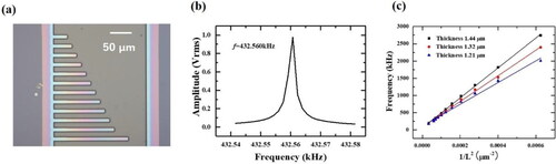
Figure 11. (a) Resonance frequency spectra with different etching durations, (b) Shift of the resonance frequency with etching durations, (c) Q factor evolution with etching durations, and (d) Ring-down curve of the SCD cantilever after 380 h etching in oxygen ambient [Citation126]. © 2018, American Physical Society.
![Figure 11. (a) Resonance frequency spectra with different etching durations, (b) Shift of the resonance frequency with etching durations, (c) Q factor evolution with etching durations, and (d) Ring-down curve of the SCD cantilever after 380 h etching in oxygen ambient [Citation126]. © 2018, American Physical Society.](/cms/asset/cbbb9eda-ff71-4cf8-8275-3be2c3a07ad4/tfdi_a_1877019_f0011_c.jpg)
Figure 12. (a) Magnetic sensing principle for diamond MEMS integrated with a magnetostrictive thin film, (b) frequency spectra with external magnetic field, and (c) shift of the resonance frequency with external magnetic field [Citation131]. © 2019, Elsevier.
![Figure 12. (a) Magnetic sensing principle for diamond MEMS integrated with a magnetostrictive thin film, (b) frequency spectra with external magnetic field, and (c) shift of the resonance frequency with external magnetic field [Citation131]. © 2019, Elsevier.](/cms/asset/a6a3055d-2c82-4653-af13-6db8c02bb1d8/tfdi_a_1877019_f0012_c.jpg)
Figure 13. (a) Resonance frequency shift with the external magnetic filed at different temperatures of the FeGa/Ti/SCD cantilever, (b) dependence of resonance frequency shift on the temperature, (c) and (d) noise level at room temperature and 500 °C, respectively [Citation133]. © 2020, American Chemical Society.
![Figure 13. (a) Resonance frequency shift with the external magnetic filed at different temperatures of the FeGa/Ti/SCD cantilever, (b) dependence of resonance frequency shift on the temperature, (c) and (d) noise level at room temperature and 500 °C, respectively [Citation133]. © 2020, American Chemical Society.](/cms/asset/ffaf51fc-8abc-48ff-bb96-c803454cc5fd/tfdi_a_1877019_f0013_c.jpg)
Table 2. Comparison of high-temperature magnetic sensors. The references inside this table can be found in Ref. [Citation133].