Figures & data
Figure 1. Schematic of the arrangement of the filament and the wafer. The thicknesses of the spacers with 0 (no spacer), 2.5, and 5 mm are tested in this work.
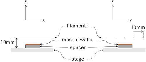
Table 1. Summary of the growth of the B-doped layers by using HFCVD in the present work.
Figure 2. (a), (b)Schematics of the is the 3-dimensional model structure, which corresponds to the actual structure for the growth experiments, and (c) mesh arrangements near the region of the voids. The voids in the calculation domain correspond to the filament. Temperature of these inner walls of these voids is set to be 2300 or 3100 °C.
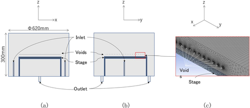
Figure 3. Pictures of the samples after the growth, which were transparent as shown in our preceding works [Citation24]. Black and red arrows represent location of the filament during the growth and the junction of the mono-crystals, which are constituents of those mosaic substrates.
![Figure 3. Pictures of the samples after the growth, which were transparent as shown in our preceding works [Citation24]. Black and red arrows represent location of the filament during the growth and the junction of the mono-crystals, which are constituents of those mosaic substrates.](/cms/asset/3bbebf77-defc-4b98-a322-52692f6d5030/tfdi_a_2068972_f0003_c.jpg)
Figure 4. Depth profiles of (a) B and (b) W measured by SIMS.
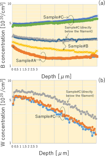
Figure 5. Raman spectra of the (a) samples #A and #B, and (c) sample#C after the growth.
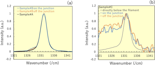
Figure 6. Profile in direction perpendicular to the line-structure of Sample#C, which was formed after the growth along with the filament.
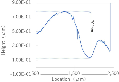
Figure 7. Global distributions of (a) gas temperature and (b) flow.
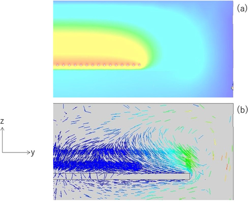
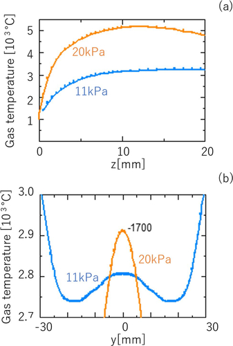
Figure 8. Profiles of the gas temperature in the (a) vertical on the axis perpendicular to the filament and (b) horizontal direction at the height 5 mm below the filament, which were calculated for the HFCVD apparatus.
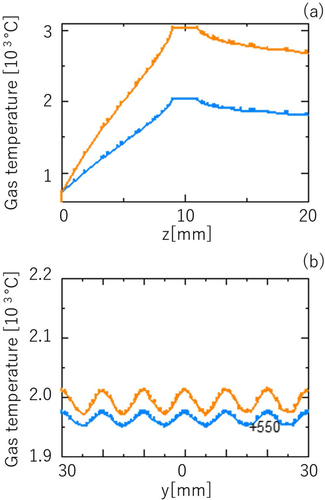
Figure 9. Profiles of the gas temperature in the (a) vertical on the central symmetric axis perpendicular to the substrate and (b) horizontal direction at the height 5 mm above the substrate top surface for the case of MWPCVD.