Figures & data
Figure 1. AFM images of diamond surface (a) without and (b) with a deposited SiC film.
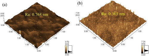
Figure 2. Optical microscopy images of the as-bonded GaN/diamond sample (a) before and (b) after removing Si substrate.
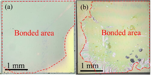
Figure 3. Respective TEM and HRTEM images taken along (a, b) the GaN zone axis and (c, d) the diamond [001] zone axis of an as-bonded GaN/diamond interface. FFT images of the interface are overlayed.
![Figure 3. Respective TEM and HRTEM images taken along (a, b) the GaN [11¯00] zone axis and (c, d) the diamond [001] zone axis of an as-bonded GaN/diamond interface. FFT images of the interface are overlayed.](/cms/asset/0a8de391-6b05-4c1b-9a27-4758487bdf33/tfdi_a_2145508_f0003_c.jpg)
Figure 4. For the as-bonded GaN/diamond interface: (a) EDS mappings; (b) X-ray intensity profiles for N, Ga, Fe, O, C, Ar, and Si atoms (shown in olive green, green, blue, red, cyan, black, and orange, respectively); and (c) enlarged X-ray intensity profiles for Fe, O, and Ar atoms.
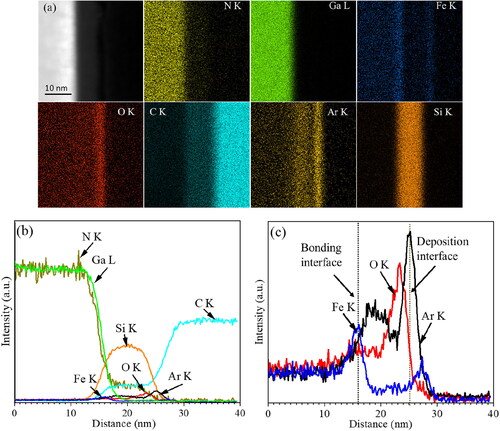
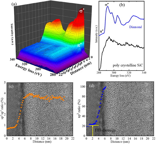
Figure 5. (a) EELS spectra line scan across the as-bonded GaN/diamond interface; (b) EELS spectra of amorphous carbon, diamond, and amorphous SiC; (c) sp2 ratios obtained from the EELS spectra as a function of the scanned distance from the interface. The overlayed TEM image in (c) indicates the corresponding positions of the scanned EELS spectra.
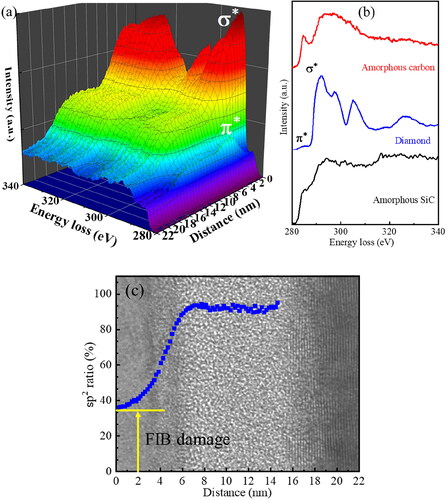
Figure 6. TEM and HRTEM images taken along (a, b) the GaN zone axis and (c, d) the diamond [001] zone axis of a GaN/diamond interface annealed at 1000 °C. FFT images at the interface are overlayed.
![Figure 6. TEM and HRTEM images taken along (a, b) the GaN [11¯00] zone axis and (c, d) the diamond [001] zone axis of a GaN/diamond interface annealed at 1000 °C. FFT images at the interface are overlayed.](/cms/asset/ca3a45ed-e07a-499d-9001-21261c59c550/tfdi_a_2145508_f0006_c.jpg)
Figure 7. For the interface annealed at 1000 °C: (a) EDS mappings; (b) X-ray intensity profiles for N, Ga, Fe, O, C, Ar, and Si atoms (olive green, green, blue, red, cyan, black, and orange, respectively); and (c) enlarged X-ray intensity profiles for Fe, O, and Ar atoms.
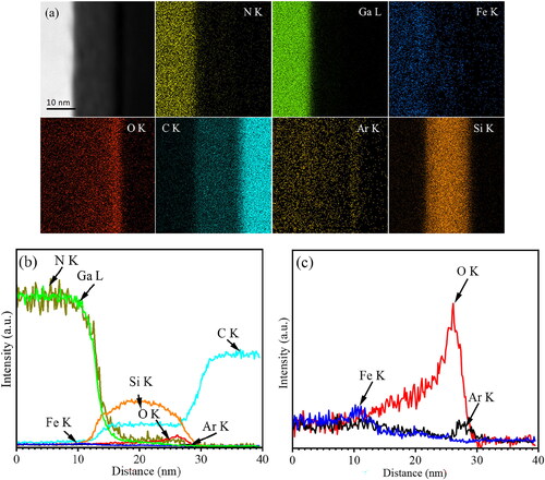
Figure 8. (a) EELS spectra line scan across the GaN/diamond interface annealed at 1000 °C; (b) EELS spectra of amorphous carbon, diamond, and amorphous SiC; (c) sp2/sp3 and (d) sp2 ratios obtained from the EELS spectra as a function of the scanned distance from the interface. The overlayed TEM images in (c) and (d) indicate the corresponding positions of the scanned EELS spectra.