
Figures & data
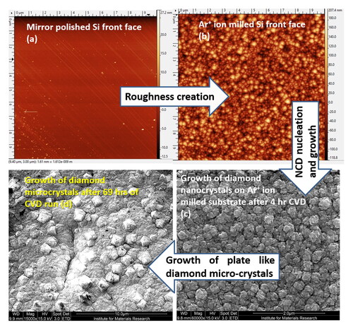
Figure 1. Microwave plasma enhanced CVD growth of diamond films inside (a) linear antenna CVD reactor, (b) resonant cavity CVD reactor, ASTeX 6500, 2.45 GHz, 3 kW.
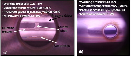
Figure 2. Profilometer scans of the substrates after surface treatments. The samples have been arranged in the increasing order of Ra surface roughness: (a) Si front face – 1.17 nm, (b) Si P4000 – 9.35 nm, (c) Si Ar+ milled – 11.29 nm, (d) Si P800 – 164.5 nm, (e) Si back face – 305.59 nm and, (f) Si P120 – Ra 1334.19 nm. (abscissa is the scan length of 5 mm and the ordinate is the average roughness expressed in nm. As every sample has different orders of roughness values, the grid line widths along the y-axis are different for all the samples. The red and green portions are, the initial and final lengths of stylus scans in mm, which were excluded during the average roughness calculations by the software.).
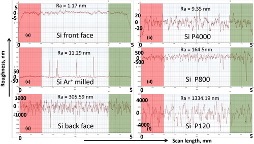
Figure 3. Effect of Si surface roughness creation by abrasion on their hydrophilicity – contact angles: (a) Si polished surface – 36º, (b) Si P4000 – 19º, (c) Si P800 – 6º and, (d) Si P120 ∼ 0º (equivalent length of the double headed arrow scale bar is 1 mm).
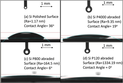
Figure 4. AFM scans of the (a) as-received silicon wafer surface, (b) argon ion milled silicon surface, (c) after 5-min resonant cavity CVD growth on the silicon surface shown in figure (a) with DND seeds, (d) Raman signals from the diamond crystals shown in figure (c).
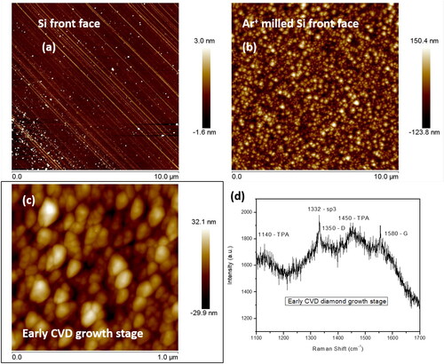
Figure 5. AFM images of DND seeded silicon substrates with seeding densities of (a) front face – 2 × 1010 cm−2, (b) back side – 6 × 1010 cm−2, (c) P4000 abraded – 5 × 1010 cm−2 and, (d) Ar+ milled – 1.2 × 109 cm−2.
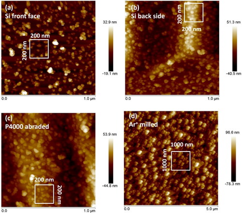
Figure 6. SEM images of CVD grown NCD on (a) mirror polished silicon surface at magnification 60KX irregular shaped grains (4 h growth); (b) regular round shape morphology NCD after 4 h growth at magnification 15KX on Ar+ ion milled substrates, (c) MCD morphology after 69 h of growth at magnification 60KX and inset figure shows 15KX magnification image, on Ar+ ion milled substrates, (d) uniform rounded NCD grains at 60KX magnification from figure (b); (e) NCD on untreated silicon wafer unpolished backside and; (f) NCD on Ar+ ion milled silicon wafer unpolished backside.
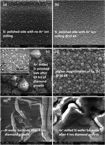
Figure 7. SEM images of the (a) MCD after 69 h CVD growth, (b) NCD after 4 h CVD growth, at 60KX magnification for silicon substrates scratched with P800 emery paper; cross-sectional images for columnar structures- (c) after 69 h CVD growth, (d) after 4 h CVD growth (e) Raman spectra for diamond films grown on scratched and unscratched wafers at different time intervals.
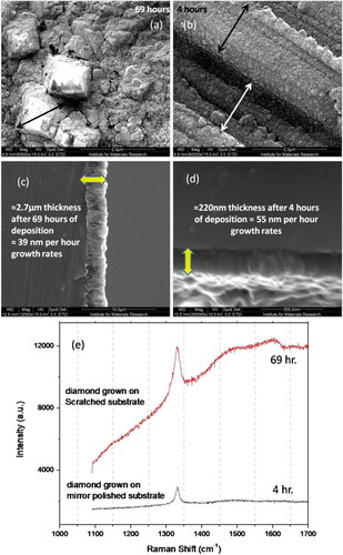
Figure 8. SEM morphologies of the NCD films on substrates (a) mirror polished silicon – 1.2 nm, (b) P4000 – 9.3 nm, (c) P1200 – 92.4 nm, (d) P800 – 164.5 nm, with different surface roughness (Ra) at identical magnification of 15KX, inside linear antenna microwave plasma enhanced CVD system. The inset images in (c) and (d) were taken at higher magnification of 60KX.
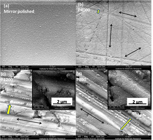
Figure 9. SEM morphologies of the NCD on scratched substrates (a) P1200 – 92.4 nm, (b) P800 – 164.5 nm, (c) P320 – 500 nm, (d) P180 – 825 nm, with different surface roughness (Ra) at identical magnification of 50KX, grown inside resonant cavity microwave plasma enhanced CVD system for 2 hrs. The inset images were taken at higher magnifications of 100KX.
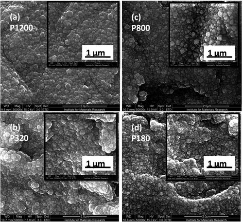
Figure 10. (a) SEM image of the diamond nanocrystals grown over P4000 abraded Si substrate after 2 h growth, (b) SEM image of the diamond micro-plates grown over mirror polished Si after 64 h growth, (c) Raman spectra of the different NCD films on substrates with different surface roughness after 2 h CVD growth, (d) cross-sectional SEM of the diamond coating shown in – all were grown inside resonant cavity microwave plasma enhanced CVD system.
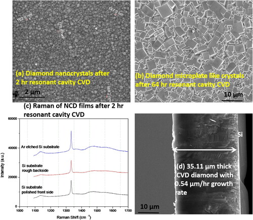
Table 1. Summary of the important experimental results.