Figures & data
Figure 1. (a) Raman spectrum and (b) FESEM image of the as-deposited nanocrystalline diamond film; (c) low-magnification TEM image of the interface region; (I) the HAADF image; (II)-(IV) EDX mapping information of Si, Ta, and C, respectively. (d) High-magnification TEM image of the interface region, corresponding enlarged images and FT images of regions 1 and 2 in (b).
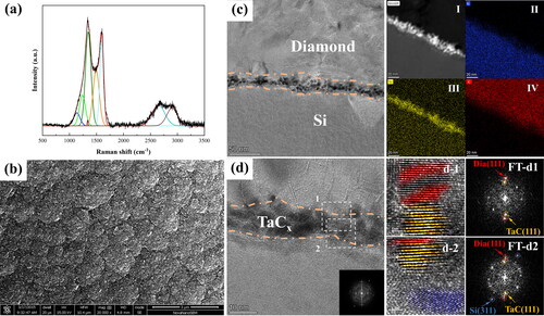
Figure 2. Side view and top view of the four different Diamond111)/TaC (111) interface models: (a) Dia-Model I, (b) Dia-Model II, (c) Dia-Model III, (d) Dia-Model IV, and the three different graphite (002)/TaC (111) interface models: (e) Gra-Model Ⅴ, (f) Gra-Model Ⅵ, (g) Gra-Model Ⅶ.
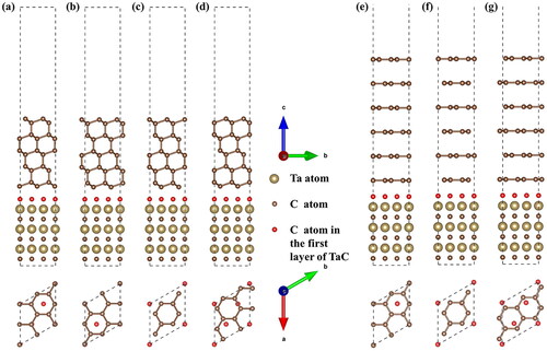
Table 1. Adsorption energy of C atom on TaC surfaces.
Figure 3. Universal binding energy relation curves of four Diamond(111)/TaC (111) interfaces and three graphite (002)/TaC (111) interfaces.
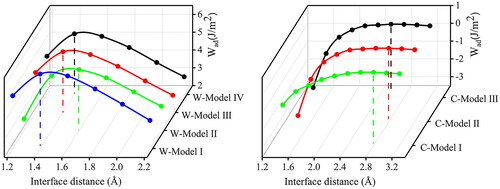
Table 2. Interface distance (d0), adhesion work (Wad) calculated using the two different methods (UBER and fully relaxation).
Figure 4. Charge density differences for fully relaxed Diamond(111)/Tac(111) and Graphite(002)/Tac(111) interfaces, (a) Relaxed-Dia-Model I; (b) Relaxed-Dia-Model II; (c) Relaxed-Gra-Model Ⅴ; (d) Relaxed-Gra-Model Ⅶ.
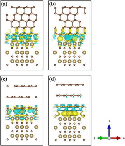
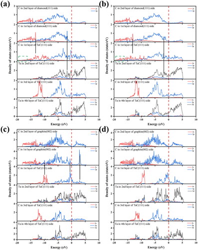
Figure 5. Partial density of states (PDOS) for fully relaxed Diamond(111)/Tac(111) and Graphite(002)/Tac(111) interfaces, (a) Relaxed-Dia-Model I; (b) Relaxed-Dia- Model II; (c) Relaxed-Gra-Model Ⅴ; (d) Relaxed-Gra-Model Ⅶ.