
Figures & data
Figure 1. AFM images of 3 C-SiC back side (a) without and (b) with polishing.
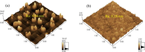
Figure 2. Process for transferring 3 C-SiC layer grown on a Si substrate to a diamond substrate.
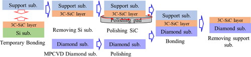
Figure 3. Optical microscopy image of the 3 C-SiC/diamond bonded sample.
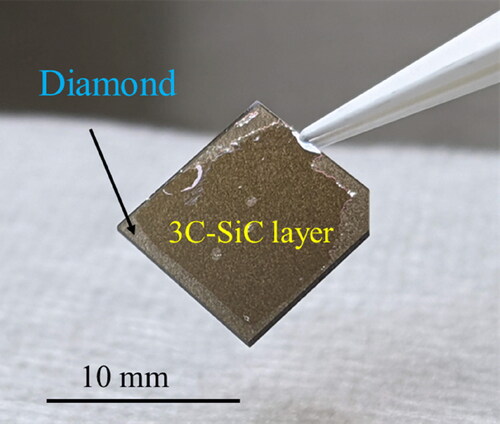
Figure 4. TEM and HRTEM images taken along the 3 C-SiC zone axis (a and b) and the diamond [001] zone axis (b and c) of an as-bonded 3 C-SiC/diamond interface. Overlaid FFT images of the interface are presented.
![Figure 4. TEM and HRTEM images taken along the 3 C-SiC [1¯10] zone axis (a and b) and the diamond [001] zone axis (b and c) of an as-bonded 3 C-SiC/diamond interface. Overlaid FFT images of the interface are presented.](/cms/asset/12c5f08b-d1bd-4966-ab28-3bd8bbf9dad0/tfdi_a_2337352_f0004_c.jpg)
Figure 5. EDS mapping of the as-bonded 3 C-SiC/diamond interface (a) and X-ray intensity profiles for C, Si, O, Ar, and Fe atoms (represented by red, blue, green, yellow, and cyan respectively) across the interface (b). The inset TEM image provides context by indicating the corresponding location of the measured X-ray intensity profiles for C, Si, O, Ar, and Fe atoms.
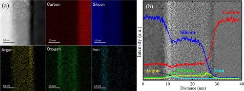
Figure 6. TEM and HRTEM images taken along the 3 C-SiC zone axis (a and b) and the diamond [001] zone axis (b and c) of a 700 °C-annealed 3 C-SiC/diamond interface. Overlaid FFT images of the interface are presented.
![Figure 6. TEM and HRTEM images taken along the 3 C-SiC [1¯10] zone axis (a and b) and the diamond [001] zone axis (b and c) of a 700 °C-annealed 3 C-SiC/diamond interface. Overlaid FFT images of the interface are presented.](/cms/asset/ffd1687e-6b3f-4b94-afbe-ff36e9966af6/tfdi_a_2337352_f0006_c.jpg)
Figure 7. EDS mapping of the 700 °C-annealed 3 C-SiC/diamond interface (a) and X-ray intensity profiles for C, Si, O, Ar, and Fe atoms (represented by red, blue, green, yellow, and cyan respectively) across the interface (b). The inset TEM image provides context by indicating the corresponding location of the measured X-ray intensity profiles for C, Si, O, Ar, and Fe atoms.
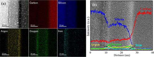
Figure 8. TEM and HRTEM images taken along the 3 C-SiC zone axis (a and b) and the diamond [001] zone axis (b and c) of a 1100 °C-annealed 3 C-SiC/diamond interface. Overlaid FFT images of the interface are presented.
![Figure 8. TEM and HRTEM images taken along the 3 C-SiC [1¯10] zone axis (a and b) and the diamond [001] zone axis (b and c) of a 1100 °C-annealed 3 C-SiC/diamond interface. Overlaid FFT images of the interface are presented.](/cms/asset/afb2abc7-d0f0-4b35-b2d6-495fb943f325/tfdi_a_2337352_f0008_c.jpg)
Figure 9. EDS mapping of the 1100 °C-annealed 3 C-SiC/diamond interface (a) and X-ray intensity profiles for C, Si, O, Ar, and Fe atoms (represented by red, blue, green, yellow, and cyan respectively) across the interface (b). The inset TEM image provides context by indicating the corresponding location of the measured X-ray intensity profiles for C, Si, O, Ar, and Fe atoms.
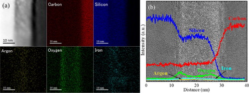
Figure 10. Density profiles of C and Si atoms (red and blue, respectively) across the as-bonded (a), 700 °C-annealed (b), and 1100 °C-annealed (c) 3 C-SiC/diamond interfaces obtained by EDS.
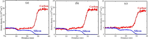
Figure 11. TDTR measurements on the diamond substrate and the 3 C-SiC/diamond sample with annealing at 1100 °C. (a) Picosecond ultrasonics measurements on the diamond substrate sample. (b) the data fitting of TDTR experimental data on the diamond substrate sample. (c) Picosecond ultrasonics measurements on the 3 C-SiC-diamond sample. (d) the data fitting of TDTR experimental data on the 3 C-SiC-diamond sample.
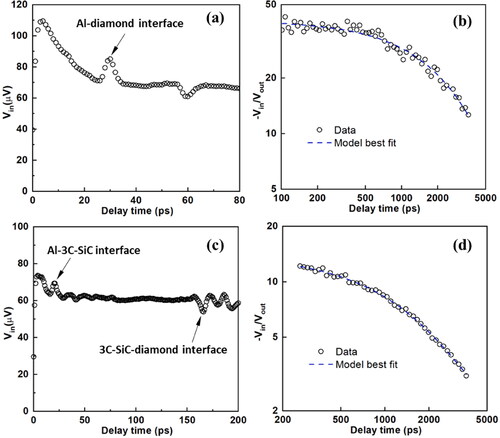
Table 1. Summary of TDTR results of the bonded 3 C-SiC-diamond sample.