Figures & data
Table 1. The summary of experimental condition variables for preferred orientation growth of diamond.
Figure 1. Surface morphology of silicon substrate after seeding (a) 5000 times and (b) 40000 times.
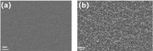
Figure 2. (a1) Grain morphology and (a2) film morphology and (a3) the transition region of discrete grains to film formation morphology of S1 sample; (b1) Grain morphology and (b2) film morphology and (b3) the transition region of discrete grains to film formation morphology of S2 sample; (c1) grain morphology and (c2) film morphology and (c3) the transition region of discrete grains to film formation morphology of S3 sample.
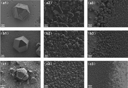
Figure 3. (a1) Grain morphology and (a2) film morphology and (a3) the transition region of discrete grains to film formation morphology of S4 sample; (b1) Grain morphology and (b2) film morphology and (b3) the transition region of discrete grains to film formation morphology of S5 sample; (c1) grain morphology and (c2) film morphology and (c3) the transition region of discrete grains to film formation morphology of S6 sample.
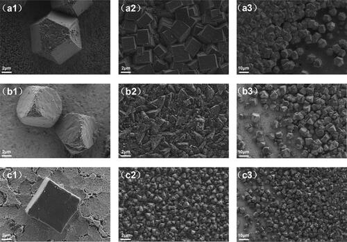
Figure 4. (a1) Grain morphology and (a2) film morphology and (a3) the transition region of discrete grains to film formation morphology of S7 sample; (b1) Grain morphology and (b2) film morphology and (b3) the transition region of discrete grains to film formation morphology of S8 sample; (c1) grain morphology and (c2) film morphology and (c3) the transition region of discrete grains to film formation morphology of S9 sample.
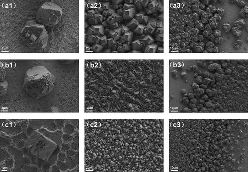
Figure 5. XRD test results (2θ mode) of (a) samples S1–S3, (b) samples S4–S6, and (c) samples S7–S9.
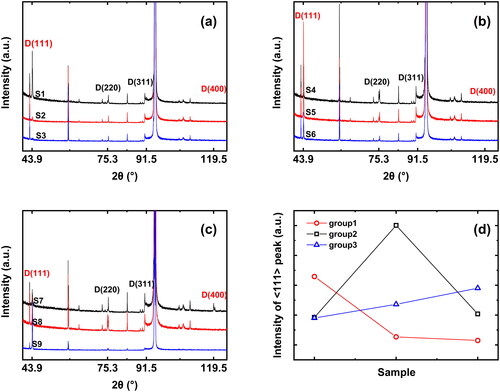
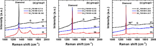
Figure 6. Raman spectrum test results of (a) samples S1–S3, (b) samples S4–S6, and (c) samples S7–S9.