Figures & data
Figure 1 (a) Illustration of structuring SC-OFETs with the method of crystal lamination. (b) A top view of the SC-OFETs with a thin laminated rubrene crystal.
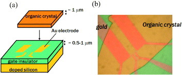
Figure 2 (a) SC-OFETs with parylene gate insulating layers. (b) SC-OFETs with vacuum-gap dielectrics.
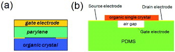
Figure 3 Schematic diagram of the four-terminal conductivity measurement with applied gate voltage in OFETs.
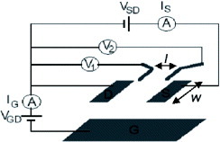
Figure 4 History of the development of high-mobility OFETs. Red open circles indicate representative values of mobility for certain years.
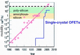
Figure 5 Molecular and crystal structures of rubrene.
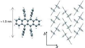
Figure 6 A molecularly flat surface extends a few tens of micrometers at the surface of rubrene crystals (an AFM image).
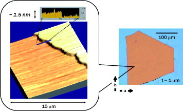
Figure 7 Transfer characteristics of rubrene single-crystal transistors fabricated on SiO2 dielectrics treated with SAMs. (a) and (b) represent the results of two-terminal and four-terminal measurements, respectively. The inset in the upper panel shows low-angle x-ray diffraction of the highly ordered SAMs, while the inset in the lower panel presents output characteristics (reproduced with permission from [Citation6]).
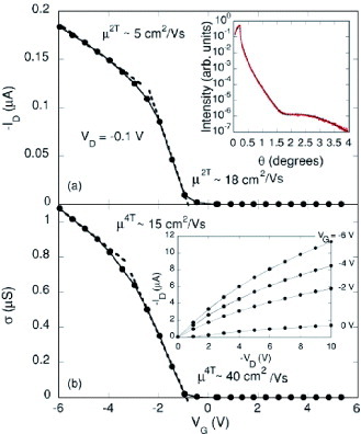
Figure 8 Output characteristics of a rubrene SC-OFET with CYTOP gate insulators. Hysteresis is negligible. Saturation mobility is estimated as high as 30 cm2 Vs−1 (reproduced with permission from [Citation40]).
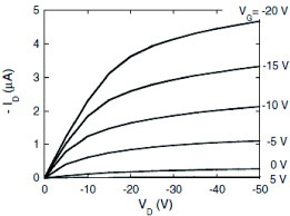
Figure 9 (a) A well structure to hold ionic liquid to form SC-OFETs with solid-to-liquid interfaces. (b) 1-ethyl-3-methylimidazolium bis(trifluoro-methyl-sulfonyl)imide [emim TFSI], as an example of an ionic liquid (reproduced with permission from [Citation49]).
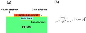
Figure 10 (a) Transfer and (b) output characteristics of the ionic liquid/rubrene SC-OFETs. Inset in (a): optical view of the device (reproduced with permission from [Citation49]).
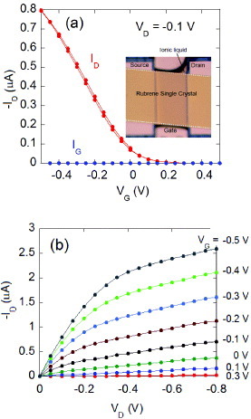
Figure 11 Molecular and crystal structures of pentacene. ‘Z’ represents the axis perpendicular to the molecular layers.
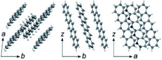
Figure 12 (a) Channel conductivity versus gate voltage at different temperatures from 160 to 260 K. (b) Field-effect mobility as a function of temperature for three different pentacene single-crystal devices (reproduced with permission from [Citation12]).
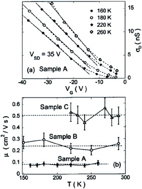
Figure 13 (a) Molecular structures of some TTF analogues studied for OFETs; (b) and (c) crystal structures of hexamethylenetetrathiafulvalene (HMTTF). Molecules at different positions along the b-axis are shown in different colors (reproduced with permission from [Citation67]).
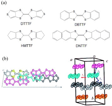
Figure 14 Transfer and output (inset) characteristics of SC-OFETs composed of single crystals grown by (a) vapor transport and (b) recrystallization (reproduced with permission from [Citation67]).
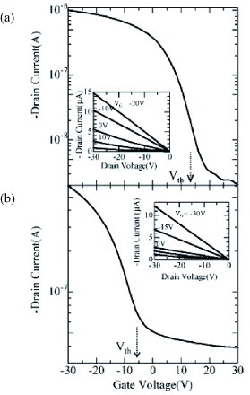
Figure 15 Left: optical view of the TCNQ SC-OTFET. Right: molecular and crystal structures of TCNQ (reproduced with permission from [Citation46]).
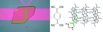
Figure 16 Transfer characteristics of typical TCNQ SC-OFETs measured with (a) two-terminal and (b) four-terminal methods. (c) Output characteristics of the TCNQ transistor (reproduced with permission from [Citation46]).
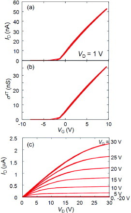
Figure 17 Molecular and crystal structure of a (DBTTF) (TCNQ) charge-transfer compound.
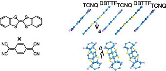
Figure 18 Transfer characteristics of DBTTF-TCNQ SC-OFETs with the source and drain electrodes composed of Au, Ag and TTF-TCNQ, measured along the b-axes (reproduced with permission from [Citation16]).
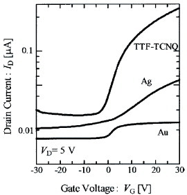
Figure 19 Schematic band diagram for lowest unoccupied conduction band (LUCB) and highest occupied valence band (HOVB) of various molecular semiconductors and the work function of inorganic and organic metals.
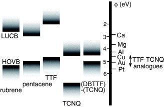
Figure 20 Transfer characteristics at VD = 5 V of DBTTF-TCNQ single-crystal field effect transistors with source and drain electrodes composed of (a) TTF-TCNQ, (b) TTF-F1 TCNQ, (c) TTF-F2 TCNQ, (d) TSF-F1 TCNQ, (e) TSF-F2 TCNQ and (f) DBTTF-F4 TCNQ measured along the crystal long axes (reproduced with permission from [Citation19]).
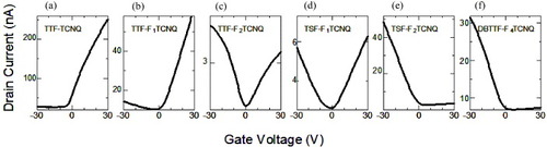
Figure 21 Schottky barrier characteristics at organic metal/semiconductor contacts. Linear (left ordinate) and Schottky barrier height (right ordinate) plotted against (IPD+EAA)/2 (fm) of the organic metals used as source and drain electrodes (reproduced with permission from [Citation19]).
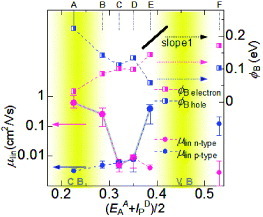
Figure 22 (a) Transfer characteristics of a rubrene single-crystal field-effect transistor at 290 K. The inset is a top view of the device. (b) Evolution of transverse voltage in a Hall bar shaped rubrene single-crystal field-effect transistor at 290 K for four different gate voltages from 25 to −175 V. The magnetic field is swept back and forth between −10 and 10 T perpendicular to the conduction channel, as shown in (c). (d) Inverse Hall coefficient and sheet conductivity plotted as a function of gate voltage at 290 K for the Hall bar shaped rubrene SC-OFETs illustrated in the inset. (e) Hall mobility as a function of gate voltage. The solid curve indicates a typical estimation of carrier-distribution depth in units of the c-axis lattice constant of rubrene. The dashed line shows the two-monolayer criterion as a guide [Citation7].
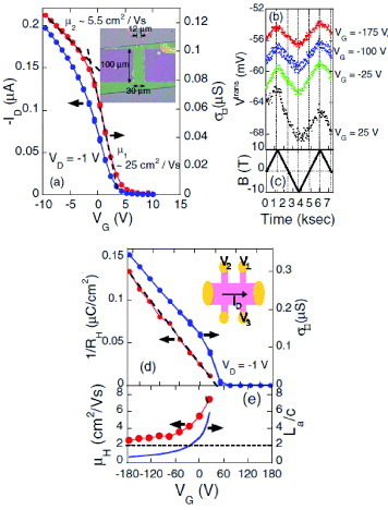
Figure 23 (a) Device structures for FI-ESR measurements. (b) Typical FI-ESR spectra of pentacene thin-film transistors (VG = - 200 V) at room temperature. (c) Temperature dependence (Arrhenius plot) of the linewidth ΔB1/2 of FI-ESR spectra at VG = - 200 V and - 100 V, and the field-effect mobility of pentacene thin-film transistors [Citation36].
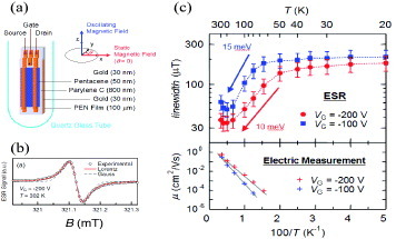
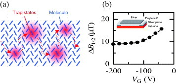
Figure 24 (a) Schematic picture of multiple trap and release (MTR) processes in a pentacene crystal. (b) Gate-voltage-dependence of ESR linewidth (HWHM) of rubrene SC-OFETs at room temperature.