Figures & data
Figure 1 TEM images showing in situ sample preparation: (a) fabrication of a W particle, (b) placement with a W tip of the particle produced in (a) on a CNT attached to a gold wire, (c) contacting the CNT with the W tip and applying bias voltage to the CNT.
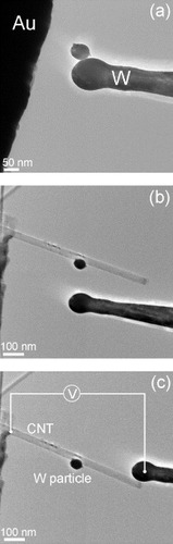
Figure 2 (a)–(e) Sequential images captured from a video (video 1 in Supplementary data available from stacks.iop.org/STAM/12/044605/mmedia) showing gradual melting of a W particle heated on the CNT. (f) Time evolution of the electric current passing through the CNT indicating the moments when images (a)–(e) were recorded. (g) Energy dispersive x-ray spectrum taken from the particle shown in (a)–(e).
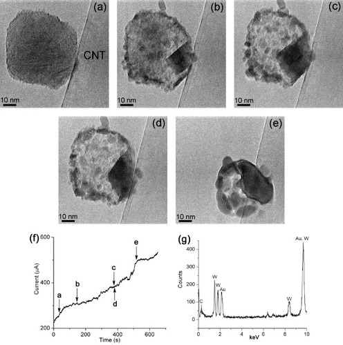
Figure 3 Diffraction patterns captured from a video (video 2 in Supplementary data available from stacks.iop.org/STAM/12/044605/mmedia) showing partial melting of a W particle heated on the CNT. (a)–(c) Patterns recorded with a period of 1 s showing rapid changes in diffraction patterns. (d)–(f) Patterns captured upon a further increase in temperature. Spots 1 and 2 correspond to a lattice spacing of 0.22 nm, in good agreement with the (110) atomic plane separation in tungsten. Also present are rings originating from the front and back parts of the CNT walls and sharp spots related to the CNT sidewalls.
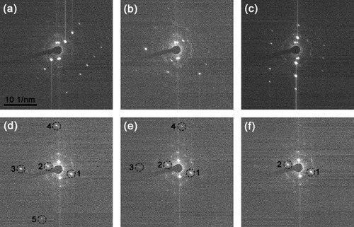
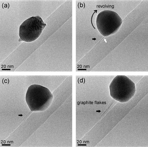
Figure 4 Sequential images captured from a video (video 3 in Supplementary data available from stacks.iop.org/STAM/12/044605/mmedia) showing the absorption of graphite layers by a melted or premelted W particle: (a) before heating. (b)–(d) After the particle was melted (or premelted), it absorbed some inner shells of the CNT (white arrow in (b)) and started rolling along the CNT, reeling off graphite layers. As indicated by black arrows in (b)–(d), a thin graphite flake grew while the particle was rolling; the flake length is ∼35, 57 and 95 nm in (b), (c) and (d), respectively.