Figures & data
Figure 1 A typical LEED pattern (a) and an Auger electron spectrum of a 0.3% C-doped Ni(111) substrate, which was annealed for surface precipitation. (c) An STM height image of various types of graphene-based nanostructures measured with a tungsten tip at room temperature in UHV (Vs=1.5 V, It=58 pA). Symbols in (c) mean rt: rough terrace, nt: nanotrench, mw: Moiré pattern, nw: nanowire and rc: reconstruction.
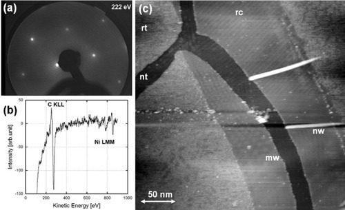
Figure 2 (a) An STM height image of a nanotrench formed in a graphite(0001) terrace on a 0.3% C-doped Ni(111) substrate, measured with a tungsten tip at room temperature in UHV (Vs=1.5 V, It=69 pA). (b) A cross-sectional profile along the white line in panel (a). The depth of the nanotrench (∼330 pm) corresponds to a monolayer height of graphite(0001) terrace.
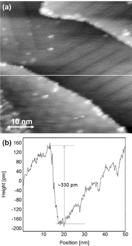
Figure 3 Height (a) and current (b) STM images of a carbon nanowire grown on a graphite(0001) terrace on a 0.3% C-doped Ni(111) substrate, measured with a tungsten tip in UHV (Vs=−1.52 V, It=0.95 nA).
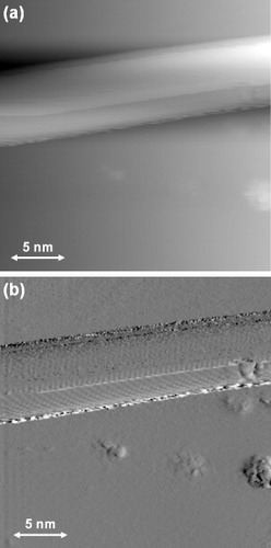
Figure 4 STM images of a 1D reconstruction pattern formed on a graphite(0001) terrace on a 0.3% C-doped Ni(111) substrate, measured with a tungsten tip (Vs=−1.5 V, It=1.1 nA). (a) An STM height image and (d) an STM current image; (b) and (e) are the FFT images of (a) and (d), respectively; (c) and (f) are the autocorrelation images of (a) and (d), respectively.
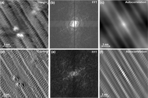
Figure 5 (a) An STM height image of Moiré pattern formed on a graphite(0001) terrace on a 0.4% C-doped Ni(111) substrate after annealing for surface precipitation, measured with a Pt–Ir tip (Vs=0.5 V, It=0.3 nA). Panel (b) is the FFT image of (a) and (c) is a simultaneously observed STM current image.
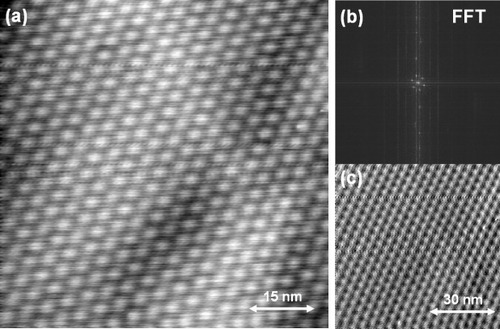
Figure 6 STM images of peculiar Moiré patterns formed on graphite(0001) terrace on a 0.4% C-doped Ni(111) substrate measured with a Pt–Ir tip. (a) STM image indicating Moiré patterns formed near a nanotrench on a graphite(0001) terrace (Vs=−0.2 V, It=0.5 nA). (b) An STM height image showing a non-uniform Moiré pattern with a varying periodicity, formed on a graphite(0001) terrace (Vs=0.5 V, It=0.5 nA). The insert is an FFT image of (b) indicating a continuously changing periodicity in reciprocal space.
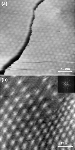
Figure 7 (a) An STM height image of graphene-based nanowires (nw) and nanobelts (nb) formed on a polycrystalline 0.4% C-doped Ni sheet, measured with a Pt–Ir tip at room temperature in UHV (Vs=0.79 V, It=0.1 nA). (b) An STM height image of a graphene nanobelt formed on a 0.4% C-doped Ni(111) substrate, measured with a Pt–Ir tip at room temperature in UHV (Vs=−0.96 V, It=0.1 nA).
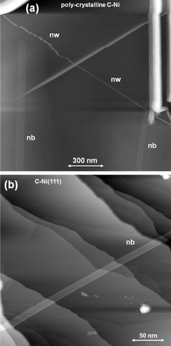
Figure 8 (a) An STM height image of a carbon nanobelt formed on a graphite basal plane of a polycrystalline C-doped Ni sheet, measured with a Pt–Ir tip (Vs=0.79 V, It=0.1 nA). (b) Cross-sectional profile along the white line in panel (a). The height of the nanobelt (∼0.8 nm) corresponds to a height of graphene bilayer.
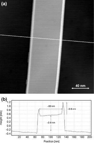
Figure 9 Scanning tunneling spectroscopy of a carbon nanobelt measured with a Pt–Ir tip at room temperature. (a) An STM height image (Vs=0.7 V, It=0.1 nA); (b) and (d) current–voltage (I–V) curves of the nanobelt and a graphite terrace; (c) and (e) differentiated (dI/dV) curves of the nanobelt and graphite terrace.
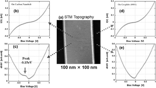
Figure 10 Schematic growth model of graphene-based nanostructures on a carbon-doped Ni(111) substrate at elevated temperatures in UHV. At high temperatures, surface carbon atoms are enriched by surface segregation up to a few atomic percent, while the majority of carbon atoms are still dissolved in the bulk. A monolayer graphene phase appears upon cooling where the surface coverage is nearly unity. Further decrease of temperature initiates surface precipitation and the growth of multilayer graphene. Graphene-based structures such as nanowires can grow at defective sites such as steps.
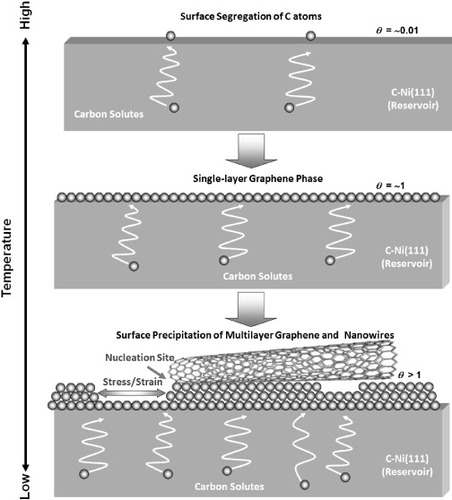
Figure 11 (a) An SEM image of a 1.0% C-doped Ni tip with a graphitic overlayer formed by surface precipitation in UHV. (b) An SEM image of a carbon nanowire protruding from the surface. (c) Auger electron spectra of the surfaces of a C-doped Ni tip before and after annealing for surface precipitation.
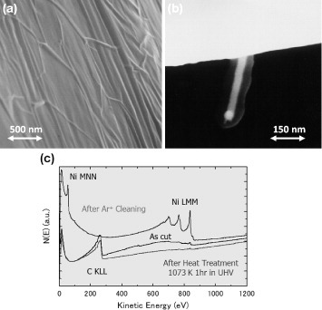
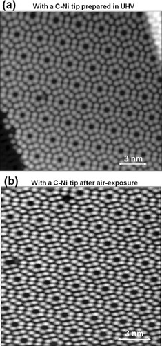
Figure 12 (a) An STM height image of an n-type Si(111) surface observed at 80 K with a 1.0% C-doped Ni tip with graphitic overlayers formed by surface precipitation (Vs=1.7 V, It=30 pA). (b) The Si(111) surface observed under the same scanning conditions after exposing the tip to air (T=301 K, humidity=59%) for 1 h.