Figures & data
Figure 1. Schematic of a mid-IR lab-on-a-chip sensor system that combines a light source, sensing elements, a detector and read-out circuitry on a monolithic silicon platform. The functionalization layer adds specificity to the sensor response for greater accuracy in analyte recognition (image courtesy of [Citation33]).
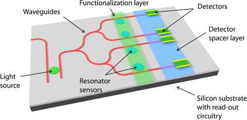
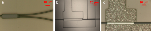
Figure 2. (a) SEM image of a silicon pedestal waveguide ([Citation32] reproduced by permission of The Royal Society of Chemistry); (b) scanning electron microscope (SEM) image of a SOUP waveguide (image courtesy of [Citation33]) and (c) mid-IR camera images showing the in situ attenuation and recovery of the waveguide mode as an absorbing analyte is introduced and then allowed to evaporate.
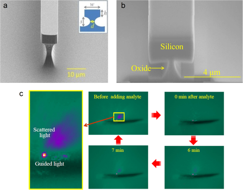
Figure 3. The waveguide mode intensities at different toluene/CCl4 concentrations. The intensities decrease as the toluene ratio increases because of mid-IR absorption from the aromatic C–H stretch in toluene at the selected wavelength λ = 3.3 μm ([Citation32] reproduced by permission of The Royal Society of Chemistry).
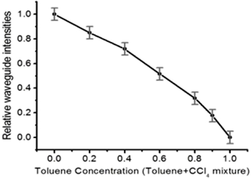
Figure 4. Chemical sensing using our fabricated on-chip mid-IR pedestal silicon waveguide sensor. Tested analytes show different absorbance at λ = 3.55 μm. Results from our measurements (red bars) are compared with those from literature (black bars) ([Citation32] reproduced by permission of The Royal Society of Chemistry).

Figure 5. (a) Captured mid-IR images and (b) intensity profiles of a SiNx directional coupler as a function of wavelength. At λ = 2.45 μm, channel 1 has maximum output, whereas the maximum of channel 2 appears at λ = 2.65 μm. Guided waves remain fundamental modes in both channels. Copyright Wiley-VCH Verlag GmbH & Co. KGaA. Reproduced with permission from [Citation35].
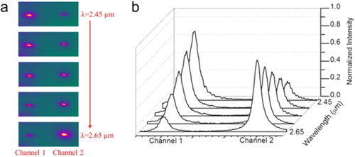
Figure 6. (a) Optical microscope image of a mid-IR microdisk resonator and (b) SEM cross-section of a single-mode mid-IR bus waveguide (images courtesy of [Citation49]).
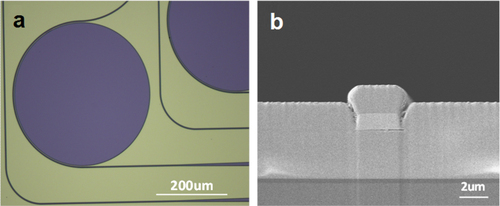
Figure 7. (a) Top view microscope image of the waveguide PhC cavity, consisting of a section of unstructured channel waveguide (∼ 170 μm in length) confined between two PhC mirrors (marked by the red boxes) and (b) top-view SEM image of one of the PhC mirrors (images courtesy of [Citation50]).
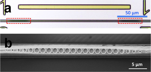
Figure 8. (a) Schematic diagram of the mid-IR fiber-end fire measurement setup (image courtesy of [Citation49]); (b) photo of mid-IR measurement set up; (c) top-view microscope image of a mid-IR InF3 fiber-end fire coupled to an Ge23Sb7S70 waveguide with a lateral taper to reduce the mode mismatch and (d) far-field image of the TE guided mode from a single-mode Ge23Sb7S70 waveguide on the CaF2 substrate.
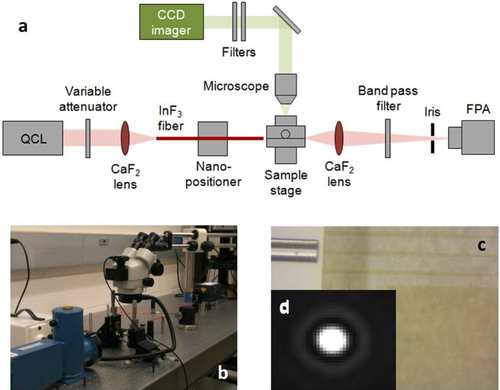
Figure 9. (a) Relative output intensity as functions of As2Se3 waveguide lengths; the widths of the waveguides are labeled in the box in the top-right corner; (b) the mid-IR optical transmission spectrum of the As2Se3 microdisk resonator measured using a wavelength sweeping method and (c) the spectrum near the optical resonance at 5157.89 nm wavelength (the red box in (b)). The dots are experimentally measured data and the line is the linear-scale Lorentzian fit, which indicates a loaded cavity quality factor of 105 (images courtesy of [Citation49]).
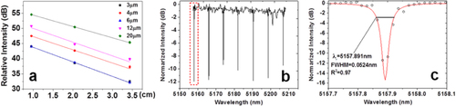
Figure 10. (a) The mid-IR transmission spectrum of a waveguide PhC cavity with two ten-hole PhC mirrors and (b) the evolution of loaded cavity Q-factors as the PhC mirror hole number increases: the black bars represent experimentally measured Q values and the red crosses denote the simulation results (images courtesy of [Citation50]).

Figure 11. (a) The mid-IR optical transmission spectrum of a 250 μm radius Ge23Sb7S70 microdisk resonator in an ethanol/cyclohexane mixture of different volume ratios and (b) the absorption loss induced by ethanol calculated from the transmission spectra.
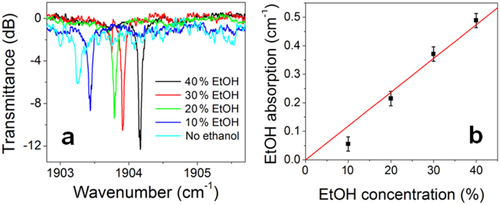
Figure 12. Scheme of layered polymers on waveguides where each layer has an affinity to a particular organic molecule or compound ([Citation60] reproduced by permission of The Royal Society of Chemistry).
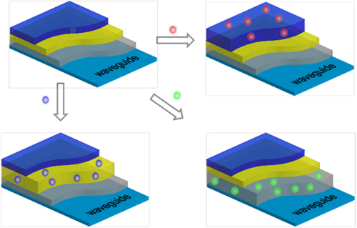
Figure 13. IR spectra of the various analyte vapors obtained with the aid of the multi-component (PGMA/PAA/EPB/PGMA/P2VP) enrichment coating deposited on the Si crystal waveguide ([Citation60] reproduced by permission of The Royal Society of Chemistry).
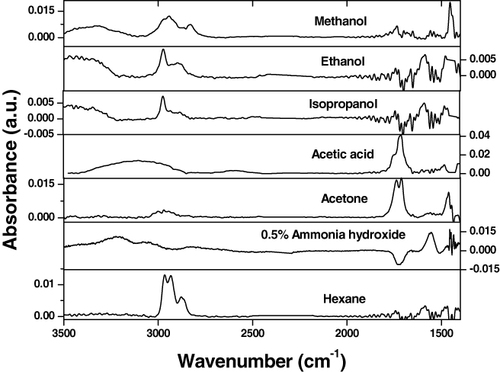
Figure 14. IR spectra of the various analyte vapors obtained with the aid of the two-component (PGMA/PAA) enrichment coating deposited on the Si crystal waveguide.

Figure 15. Atomic force microscopy (AFM) topographical images of: the initial PGMA layer and PMMA–PGMA layers; the change in the layers’ morphology upon foaming; and the collapsed layers’ morphology upon exposure to chloroform vapor. Image size: 1 × 1 μm, vertical scale: 30 nm.
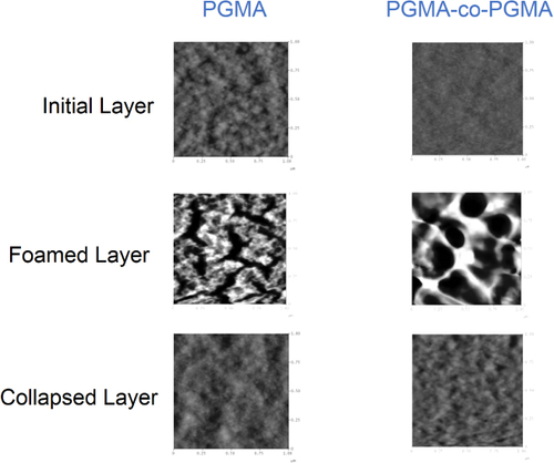
Figure 16. AFM topographical images of: the initial PGMA–PS layer and PMMA–PGMA–PS layers; the change in the layers’ morphology upon foaming and the collapsed layers’ morphology upon exposure to chloroform vapor. Image size: 1 × 1 μm, vertical scale: 30 nm.

Figure 17. (a) Integrated structure with a single-mode (λ = 3.2 μm) As2Se3 waveguide, Ge23Sb7S70 glass undercladding to prevent leakage of the mode into the Si substrate, a low index spacer to minimize modal mismatch and Fresnel reflection, and the photoconductive PbTe layer. (b) The cross-section view of the device. Reproduced with permission from [Citation96].
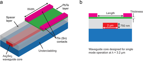
Figure 18. 3D FDTD simulations of the integrated device at λ = 3.2 μm for a 100 nm thick PbTe layer. The side (YZ) cross-section views presented for three different spacer layers exhibit the flexibility of the proposed design: all three materials allow for a gradual absorption of light in the PbTe layer with minimal reflections.
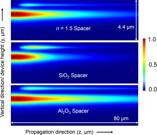
Figure 19. (a) MMI waveguide prior to spacer layer deposition; (b) resist pattern for metal contacts aligned to the PbTe layer and (c) final device after metal deposition.