Figures & data
Figure 1 Schematics of various slow-light structures producing optical delays.
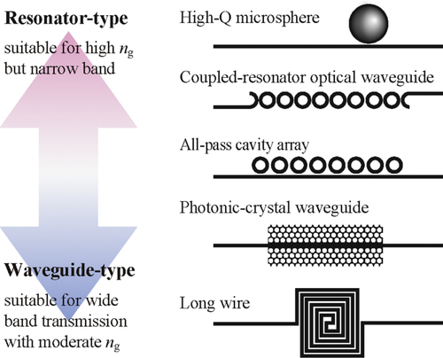
Figure 2 Slow-light enhancement in a photonic crystal waveguide. (a) Schematics of an MZ modulator based on the photonic crystal waveguide and band diagram. (b) Theoretical estimation of L π with n g, which is calculated from a simple formula for the phase shift Δø = k 0 n g(Δn/n)L where k 0 is the wave number in vacuum.
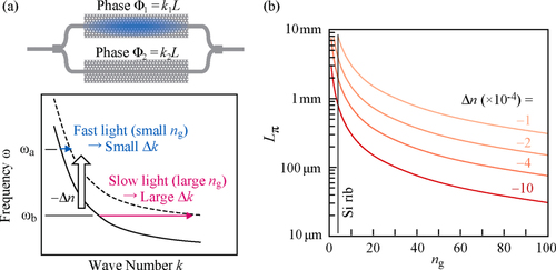
Figure 3 Fabrication of photonic crystal devices using Si photonics CMOS-compatible processes [Citation3].
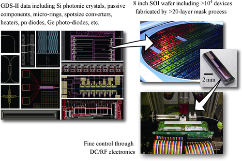
Figure 4 Si-photonic-crystal slow-light-waveguide MZ modulator (first generation). (a) Schematic. (b) Photograph of a fabricated device (right). The scanning electron microscopy image (left) was taken after removing the silica cladding. These figures are partly reproduced from [Citation13].
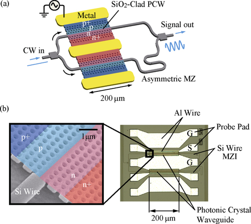
Figure 5 Photonic crystal waveguide. (a) Schematic structure. (b) Band diagram. (c) Transmission and n g spectra measured for MZ interferometer with photonic crystal waveguides [Citation13].
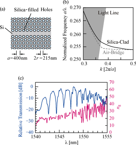
Figure 6 Performance of photonic crystal slow-light MZ modulator (first generation) [Citation13]. (a) Frequency response for sinusoidal small signal. (b) Eye patterns of pre-emphasized drive signal (left) and output signal (right) at 10 Gbps.
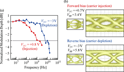
Figure 7 Si photonic crystal slow-light waveguide MZ modulator (second generation) [Citation17]. (a) Schematic. (b) Photograph of fabricated device.
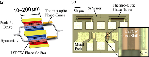
Figure 8 LSPCW. (a) Schematic structure. (b) Band diagram [Citation8]. (c) Transmission and n g spectra for different shift s [Citation18].
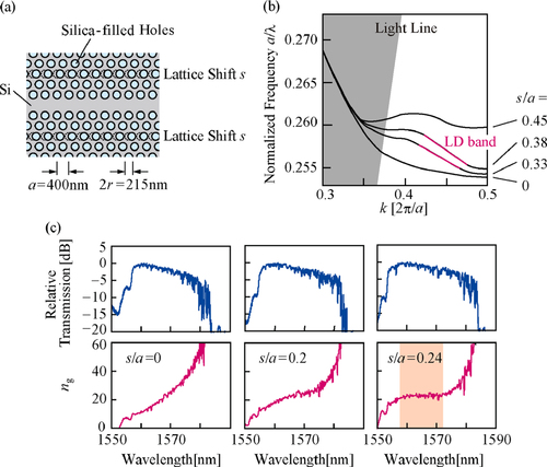
Figure 9 Slow-light enhancement in LSPCW. (a) Schematics of photonic crystal waveguide MZ modulator and band diagram. (b) Theoretical relation between Δλ and n g simply calculated from the relation Δn = n g(Δλ/λ) at λ = 1.55 μm.
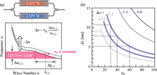
Figure 10 Modulation characteristics measured at 10 Gbps from a slow-light MZ modulator (second generation) based on a Si photonic crystal. (a) Eye patterns for various L. (b) BER characteristics [Citation18]. (c) Dependence of BER on PRBS bit length.
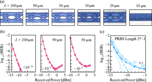
Figure 11 Modulation characteristics measured at 10 Gbps from a 200-μm-long slow-light MZ modulator (second generation) based on a Si photonic crystal. The details of the device and measurement setup are the same as those in [Citation18] except the device length.
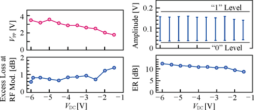
Figure 12 Wavelength (a) and temperature (b) tolerance at 10 Gbps modulation [Citation18].
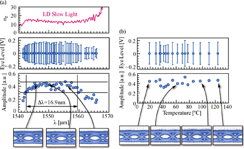
Figure 13 Single-type slow-light MZ modulator based on Si photonic crystal [Citation17]. (a) Schematic structure. VOA stands for variable optical attenuator. (b) Transmission spectrum. The color plot is taken by changing the heating power of the thermo-optic phase tuner.
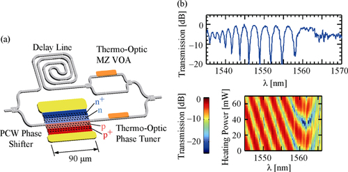
Figure 14 Eye patterns of single-type slow-light MZ modulator based on Si photonic crystal [Citation18]. (a) 25 Gbps. (b) 40 Gbps. Insets are those of electrical signals from PPG. For (a), a different sampling oscilloscope was used. Since its integration speed is lower, the pattern looks slightly noisy.
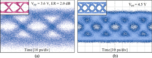
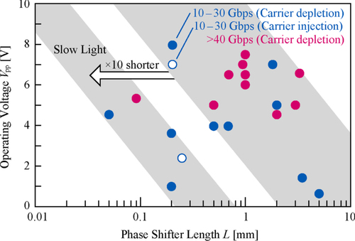
Figure 15 Operating voltage versus phase shifter length characteristics in Si MZ modulators reported so far. This figure was reproduced from [Citation17].