Figures & data
Figure 1 Schematic classification of polymer and dendrimer emissive materials.
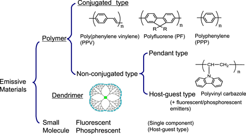
Figure 2 Solubilized emitters of dithienyl benzothiadiazole derivatives [Citation7].
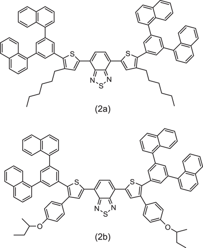
Figure 3 Copolymerization structure of functional units of a typical light-emitting polymer.
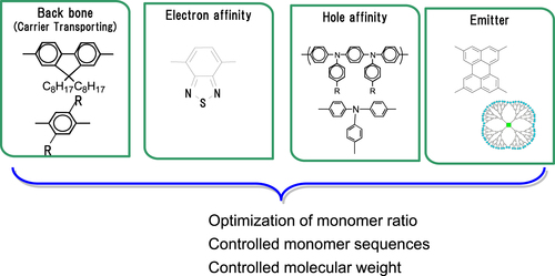
Table 1 EL emission color of fluorene-acene copolymers [Citation25].
Table 2 Comparison of characteristics between small molecule type and polymer type OLED.
Figure 4 The dependence of (a) hole mobility and (b) the current efficiency of EL devices on the content of hole transporting units in light emitting polymers [Citation36].
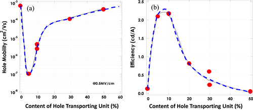
Figure 5 (a) EL efficiency at an internal electric field (0.3 MV cm−1) of ITO/PEDT:PSS (65 nm) ∕ F 8 BT (x nm) ∕ Ca (5 nm) ∕ Al (400 nm) LEDs with/without the TFB interlayer as a function of F8BT film thickness, (b) Current–voltage–luminance and (c) EL efficiency-voltage characteristics of LEDs (x = 50 nm). Schematic of the device structure and the chemical structures of TFB and F8BT are shown. F8BT is a highly luminescent semiconducting polymer that emits green–yellow light, and has a large ionization potential (5.8 eV) and a large electron affinity (2.95 eV). (Reprinted with permission from [Citation38], ©2005 American Institute of Physics.)
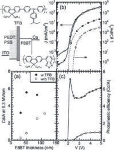
Figure 6 Degradation curves of EL and PL peak intensities of EL device containing a blue polymer during constant-current operation. Device structure: ITO/ HIL/ IL(20 nm)/ LEP(60 nm)/ cathode.
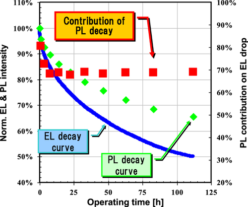
Figure 7 PL spectra of OLEDs before and after they were operated at 25 mA cm−2 for 130 h: (a) hole-driven device and (b) electron-driven device.
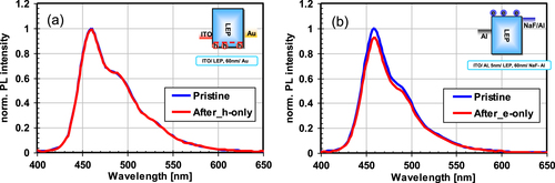
Figure 8 (a) Chemical structures of the materials under study. (b) External quantum efficiency of a prototypical PLED device comprising an F8-PFB LEP and a TFB interlayer, without (▪) and with (•) the addition of the triplet quenching additive (3). (Reprinted with permission from [Citation41], ©2011 American Institute of Physics.)
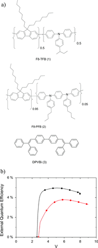
Figure 9 The decay of the device luminance (upper panel) with time and the change in efficiency of the device with time (lower panel) for a standard device (solid line) and a device containing the triplet quenching additive (dashed line). The devices were both driven from a starting luminance of 5000 cd m−2. (Reprinted with permission from [Citation41], ©2011 American Institute of Physics.)
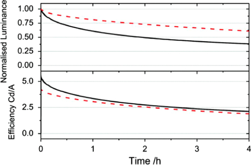
Figure 10 Process of formation of singlet and triplet excitons in the electroluminescence process (from figure [Citation53]).
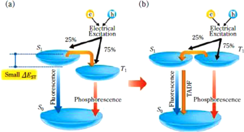
Figure 11 The current–voltage curve and the parameters of solar cell.
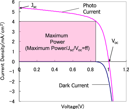
Figure 12 Device structure of bulk hetero type and mechanism of charge separation.
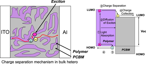
Figure 13 Examples of highly efficient p-type polymers.
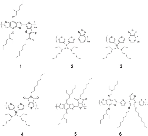
Table 3 Examples of OPV performances of long-wavelength absorption polymers.
Figure 14 Concept of molecular design for narrow band gap polymers.
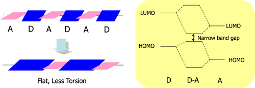
Figure 15 Chemical structures of polymer donors (PTPD3T, PBTI3T) and fullerene acceptor (PC71BM) [Citation75].
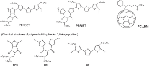
Table 4 Optimized photovoltaic response data for PTPD3T:PC71BM and PBTI3T:PC71BM inverted BHJ [Citation75].
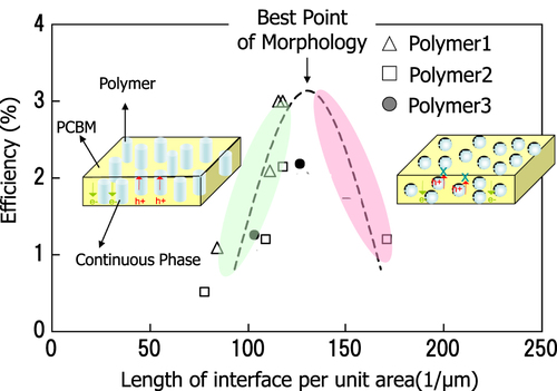
Figure 16 Relation between morphology and efficiency.