
Figures & data
Figure 1 (a) Structure model of the-Al
Pd
Mn
orthorhombic phase according to Boudard et al [Citation28]. Flat (F) and puckered (P) layers are stacked along the pseudo-tenfold direction (b axis). (b) STM image (100 × 100 nm
) of the pseudo-tenfold surface of the
-Al
Pd
Mn
[Citation26]. The terraces are covered by dots of bright contrast which are identified as decagonal rings of Al atoms decorating the unit cell as shown in the image (10 × 10 nm
) in (c). The yellow (white) rectangles give the surface unit cell dimensions [Citation26].
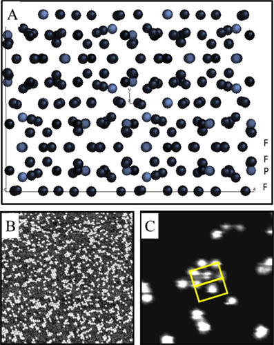
Figure 2 (a), (b) 4 nm × 4 nm high resolution STM images recorded on two different regions on the same surface. (c), (d) A tiling used to describe the puckered layer (P) has been superimposed on both STM images. While positioned identically with respect to the tiling, the contrast within the largest pentagons varies drastically within the same image and between both images of opposite bias [Citation30]. Reprinted with permission from [Citation30]. Copyright (2010) by the American Physical Society.
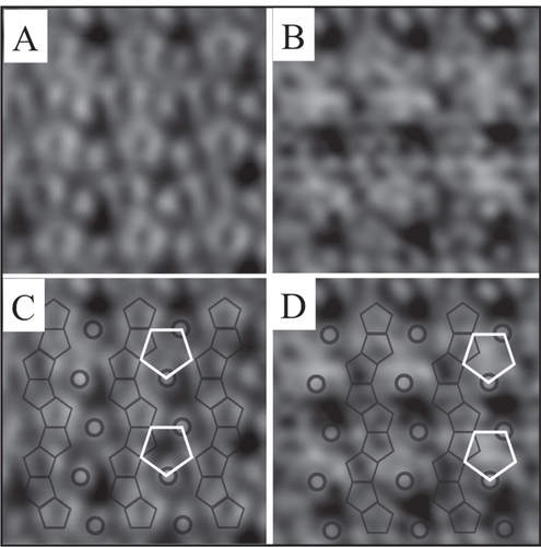
Figure 3 (a) Representation of the μ-AlMn structure along the [001] direction from [Citation34]. LEED patterns obtained on the μ-Al
Mn(001) surface at (b) 21 eV and (c) 57 eV [Citation35]. (Figures (b), (c) from [Citation35], reprinted by permission of Taylor
Francis Ltd, www.tandfonline.com.)
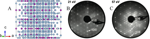
Figure 4 (a) STM image (300 Å × 300 Å) revealing terraces on the Al(Cr,Fe)(100) surface. The step height is measured at 5.8 ± 0.2 Å. (b) Structural model demonstrating the inversion symmetry of adjacent terraces [Citation37]. (Figure reproduced from [Citation37] with permission from Oldenbourg Wissenschaftsverlag, München).
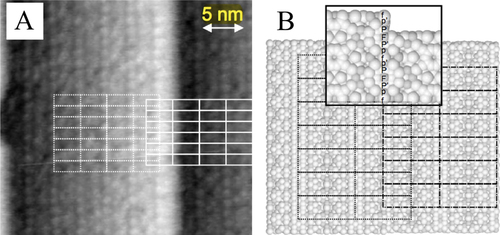
Figure 5 (a)–(e) STM images showing respectively the twofold d-Al-Ni-Co(12110) surface at 5.4 K and the Y-Al-Ni-Co(100) surface (A-type termination) at 5.7 K. (b), (c), (f) Spatially resolved maps of the background-subtracted differential conductance recorded along the quasiperiodic direction and the c-axis with different set points. (d), (g) These two graphs exhibit the averaged differential conductance spectra recorded on and between columns and the total averaged spectrum [Citation43]. (Figure reproduced from [Citation43], © IOP Publishing Deutsche Physikalische Gesellschaft. CC BY-NC-SA.)

Figure 6 (a), (b) Experimental XPD images recorded for both emitters (Al 2s and Co 2p
) measured on the p-10f surface of the Al
Co
crystal with an Al Kα x-ray source. (c), (d) Single scattering cluster simulations performed for both emitters using a cluster of 3016 atoms derived from the bulk model [Citation46]. (e) Surface layer resulting from the simulated cleavage experiment. Dashed lines indicate two PB clusters. The strong and partially covalent vertical Co–Al–Co bonds between the tips of the PB clusters are indicated by red (the darkest) stripes. The P plane splits into two complementary parts, which are separated by a vacuum layer. The highly corrugated surface layer is refereed to as the Z termination in [Citation49]. (Reprinted figures with permission from [Citation46] and [Citation49]. Copyright (2009, 2011) by the American Physical Society.)
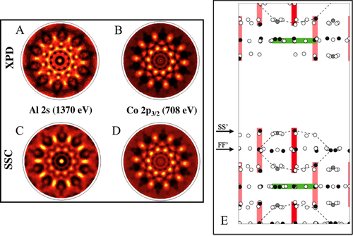
Figure 7 (a) Representation of the puckered (P) layer present in the AlFe
bulk structure. The black and gray atoms correspond to Al atoms forming pentagonal motifs. The red atoms are denoted ‘glue’ Al atoms. The empty and hatched circles are associated with Fe atoms located below and above the mean P plane position respectively. The irregular hexagon is obtained by connecting protruding Fe atoms. (b) Three-dimensional representation of the crystal structure where Fe–Al–Fe groups (host) encapsulated within Al cavities (cages) have been displayed. (c) 5 nm × 5 nm high resolution STM image (V
= −1.05 V) after annealing the Al
Fe
(010) surface to 873 K. (d) Simulated STM image (V
= −1 V) for an incomplete P layer that preserves the pentagonal bipyramid clusters at the crystal surface. (e) Electronic density of states calculated for the surface and subsurface layers of the Al
Fe
[Citation55]. (Reprinted figure with permission from [Citation55]. Copyright (2013) by the American Physical Society.)
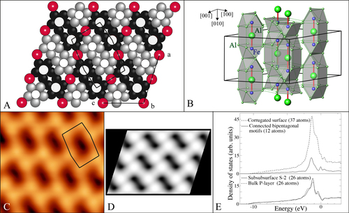
Figure 8 Top row: STM images of the AlCu
(110) surface showing the two puckered planes identified across terraces. Bottom row: simulated STM images obtained at V
= +0.5 V for the PP (a) and PF (b) models. (c) Representation of the bulk structure along the [110] direction [Citation59]. (Reprinted figure (a), (b) with permission from [Citation59]. Copyright (2010) by the American Physical Society.)
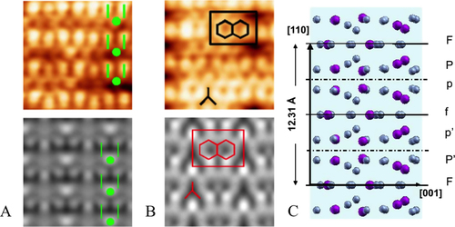
Figure 9 (Left) Bulk structure of the AlCo
crystal where the single-capped square antiprismatic clusters have been highlighted. The large (small) spheres correspond to Co (Al) atoms. (Middle) STM image of the (001) surface simulated at 1.3 V for an Al-rich plane. (Right) Experimental STM images recorded on the Al
Co
(001) surface for V
= −1.3 V, I
= 0.36 nA [Citation66]. (Reprinted figure with permission from [Citation66]. Copyright 2011 American Chemical Society.)
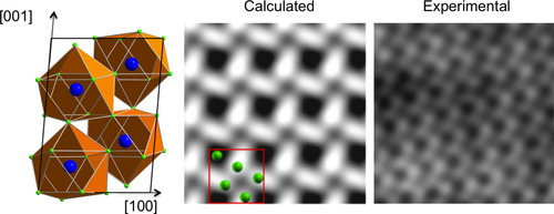
Figure 10 (a) View of the (001) plane without Cu atoms. (b) Graphite-like aluminium planes parallel to the [110] direction. (c) LEED pattern recorded for the AlCu(001) surface revealing the
surface reconstruction with two domains rotated from each other by
. (d) 20 nm × 20 nm high resolution STM image showing the atomic rows separated by two main spacings (L and M) and the two domains rotated by 90
from each other. The spacing S between two consecutive vacancies (highlighted as diamonds) is measured at 8.5 Å. Constant current simulated STM images using (e) 17 Å and (f) 13 Å wide row surface model at a contour of ρ = 3.7 10
e/Å
and ρ = 7.2 10
e/Å
respectively [Citation69]. (Reprinted figure with permission from [Citation69]. Copyright (2012) by the American Physical Society.)

Figure 11 (a) 20 nm × 20 nm high resolution STM image showing the AlCo
(100) surface after deposition of 0.38 monolayer equivalent (MLE) Pb adatoms at 300 K. The frame indicates the Pb row structure that initially propagates along the [010] direction. (b) Simulated STM image (V = −0.5 V) of the Pb rows aligned along the [010] direction at a coverage of 0.4 MLE. The unit cell has been highlighted. The largest spheres correspond to Pb adatoms while the others are Al atoms belonging to the protruding (dark blue/black) or buried (light blue/small grey spheres) bipentagonal motifs. The two Al glue atoms are represented by the smallest spheres (light gray). (c) 18 nm × 18 nm STM image obtained for a complete Pb ML deposited at 573 K on the surface. The structure is composed of irregularly shaped pentagonal features. (d) Tiling using irregular pentagons of a region (7.25 nm × 7.25 nm) extracted from the STM image presented in (c). The surface structure can be described as interconnected bipentagonal motifs (see white pentagons). To analyse the ML formed, the structure of the P plane (bipentagonal motifs pointing in two directions and glue atoms) has been superimposed on the Pb structure [Citation76]. (Figures reproduced from [Citation76], © IOP Publishing
Deutsche Physikalische Gesellschaft. CC BY-NC-SA.)
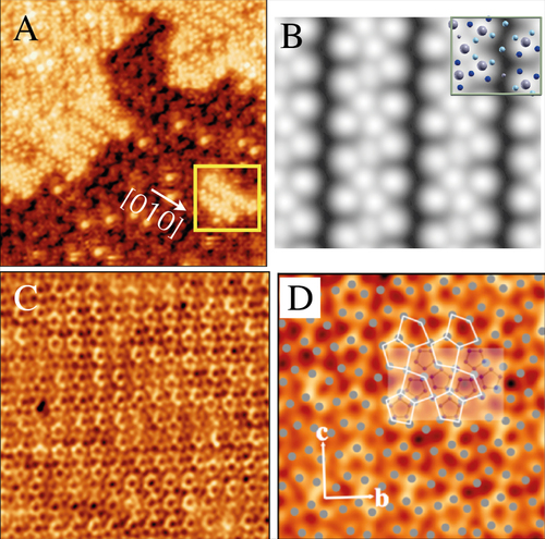
Figure 12 60 nm × 60 nm tunnelling current image of 5 ML of Bi adatoms deposited on the AlCo
(100) surface and imaged at 57 K. The boundaries between the Bi(110) (Type I) and Bi(111) (Type II) structures are indicated by dashed lines. The two insets show atomic resolution images of the structures present in Type I and II domains [Citation82]. (Figure adapted from [Citation82]. Copyright (2012) by the American Physical Society.)
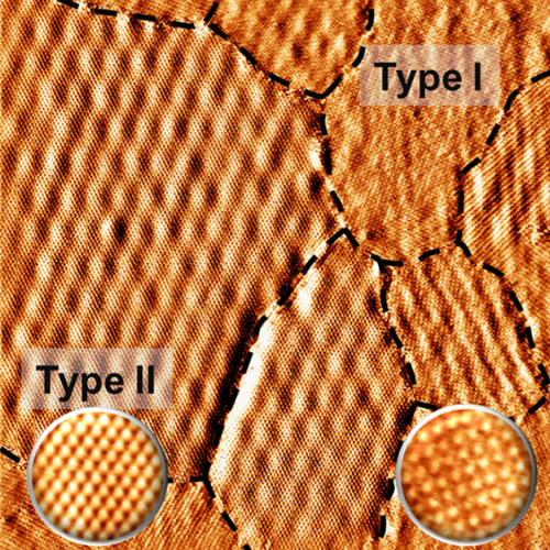
Figure 13 (a) LEED pattern (60 eV) obtained for 10 ML Cu deposition with the sample held at 473 K. The unit cell of the two domains are outlined. (b) 6 nm × 6 nm Fourier-filtered STM image showing the atomic structure of the γ-AlCu
phase. SSC simulations for (c) the Al 2s (E
= 1370 eV) and (d) the Cu 2p (E
= 1166 eV) core levels. (e) SSC pattern generated by additive superposition of the SSC simulation displayed in (b) with itself rotated by 72
. (f) XPD pattern obtained for the Cu 2p core level after 15 ML coverage [Citation85]. (Figures reproduced from [Citation85], © IOP Publishing. Reproduced with permission. All rights reserved.)
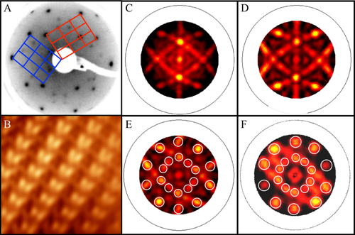
Table 1 Activation energies (, in
) of a few elemental steps involved in the hydrogenation of acetylene and desorption energy
, in
) of the C
H
molecule.
Figure 14 (a) Representation (slice cuts) of the charge density distribution prior and after oxygen adsorption. (b) 9.6 nm × 12.1 nm STM image of the AlCo
(001) surface after 0.5 L O
dosage. (c-d) Simulated STM images with atomic oxygen adsorbed on the two most energetically favourable bridge sites. The red (grey) arrows point to the adsorbed oxygen atom [Citation91]. (Figures reproduced from [Citation91] © IOP Publishing. Reproduced with permission. All rights reserved).
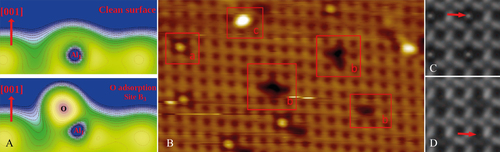
Table 2 Summary of main systems reported in this topical review.