Figures & data
Figure 1. (a) Raman Spectrum of SLG. Lorentzian curve fitting of (b) BLG and (c) TLG. (d) Comparative Raman spectra of pristine SLG, BLG and TLG. Insets in a, b and c show SEM images of SLG, BLG and TLG devices.
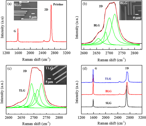
Figure 2. Raman spectra of (a) pristine and KNO3-doped SLG, (c) pristine and KNO3-doped BLG and (e) Pristine and KNO3-doped TLG. (b), (d) and (f) depict the absence of D peak of pristine and KNO3-doped SLG, BLG and TLG, respectively. The colors coding of panels a, c and e are same as panel b, d and f, respectively.
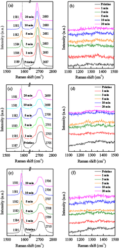
Figure 3. (a) Ratios of intensities of SLG, BLG and TLG as function of reactions time. (b) Full width at half maxima (FWHM) of 2D band of Raman Spectra of SLG, BLG and TLG as a function of reaction time.
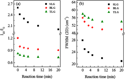
Figure 4. Resistivity as a function of back gate voltage (Vg) for (a) SLG before and after KNO3 treatment for different reaction time, (b) BLG before and after KNO3 treatment for different reaction time and (c) TLG before and after KNO3 treatment for different reaction time.
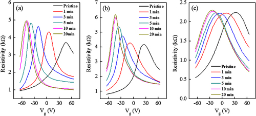
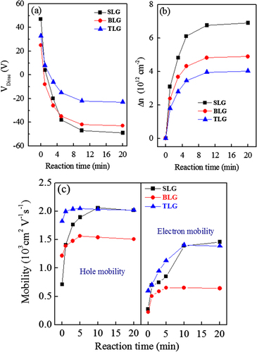
Figure 5. (a) Shift in Dirac point positions of SLG, BLG and TLG devices as a function of reaction time. (b) Change in charge density (Δn) as a function of KNO3 reaction time for SLG, BLG, and TLG. (c) The electron and hole mobility as a function of KNO3 reaction time for SLG, BLG, and TLG.