Figures & data
Figure 1 W nanowhisker arrays fabricated on the surface of an Al2O3 substrate by EBID. The intensity of the EB was 4.7×10¹⁸ e cm−2 s−1 (0.75 A cm−2) and the irradiation time was 120 s. (Reproduced with permission from [Citation18], © 2005, Springer Science+Business Media.)
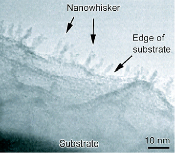
Figure 2 W nanobushs fabricated on the surface of an Al2O3 substrate by EBID. The intensity of the EB was 4.7×10¹⁸ e cm−2 s−1 (0.75 A cm−2) and the irradiation time was 19 min. (Reproduced with permission from [Citation19], © 2005, Blackwell.)
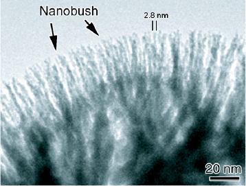
Figure 3 Arrays of W nanodendrites fabricated on the surface of an Al2O3 substrate by EBID. The intensity of the EB was 2.0×10¹⁹ e cm−2 s−1 (3.2 A cm−2) and the irradiation time was 30 s (a) A micrograph showing that the nanodendrites only grow on the convex surfaces indicated by A and B, (b) an enlargement of part of (a), showing the detail of the nanodendrites. (Reproduced with permission from [Citation18], © 2005, Springer Science+Business Media.)
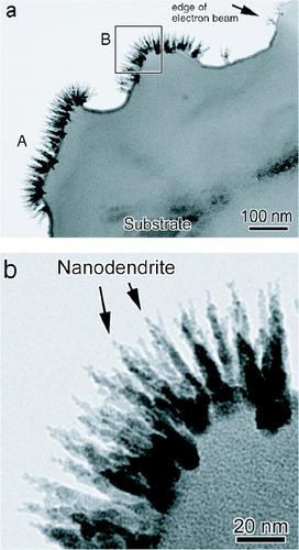
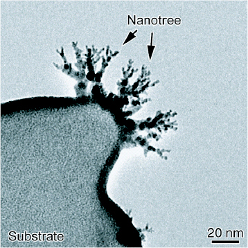
Figure 4 Fractal-like W nanotrees fabricated on the surface of an Al2O3 substrate by EBID. The intensity of the EB was 1.1×10²⁰ e cm−2 s−1 (17.9 A cm−2) and the irradiation time was 10 s. (Reproduced with permission from [Citation18], © 2005, Springer Science+Business Media.)
Typical conditions for the growth of W nanostructures on Al2O3 substrates by EBID using a 200 keV EB.
Figure 5 W nanodendrites fabricated by EBID on a sample with a hole and a convex surface. (a) The micrograph of the area before EBID; (b) the micrograph of the area after EBID. The intensity of the EB was 3.1×10¹⁹ e cm−2 s−1 (5.0 A cm−2) and the irradiation time was 10 s; (c) a schematic drawing of the charge distribution during EBID in the EB-irradiated area. (Reproduced with permission from [Citation26], © 2005, Elsevier.)
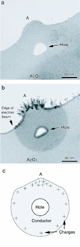
Figure 6 W nanodendrites fabricated on an Al2O3 substrate by EBID observed with different tilting angles of the substrate; (a), (b) and (c) are micrographs with the substrate tilted at −20°, 0° and 20°, respectively. The EBID is performed when the substrate is untilted.
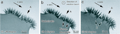
Figure 7 Schematic drawings showing the process of growth of nanostructures with different morphologies on insulator substrates by EBID. The dark dots represent the nonvolatile fraction of the precursor and the deposit, while the brighter dots represent the volatile fraction of the precursor. (a) The growth of nanowhiskers (or nanowires) inside the area of irradiation with a weak EB; (b) the growth of nanodendrites on a convex surface under irradiation with a moderate EB; and (c) the growth of fractal-like nanotrees on a convex surface under irradiation with a strong EB. (Reproduced with permission from [Citation18], © 2005, Springer Science+Business Media.)
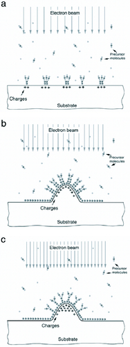
Figure 8 An x-ray EDS spectrum obtained from W nanodendrites fabricated on an Al2O3 substrate. (Reproduced with permission from [Citation18], © 2005, Springer Science+Business Media.)
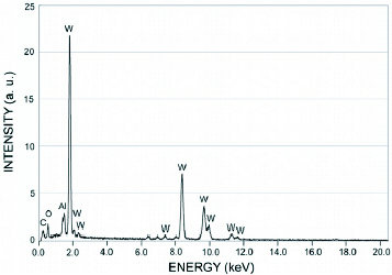
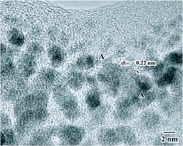
Figure 9 An HRTEM micrograph (a) and an SAED pattern (b) of W nanodendrites fabricated on an Al2O3 substrate. The arrows in (a) indicate lattice fringes in grains A and B, which have interfringe angles of 60° (A) and 90° (B), respectively. The diffuse rings in (b) correspond to the lattice spacing of bcc W crystals. (Reproduced with permission from [Citation18] © 2005, Springer Science+Business Media.)
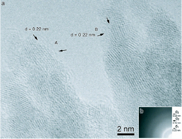
Figure 10 (a) A bright-field TEM image of as-fabricated Pt nanoparticle/W nanodendrite composite structures on an Al2O3 substrate, (b) the HRTEM image, (c) the SAED pattern, and (d) the EDS spectrum taken from the tip of the composite nanostructures. (Reproduced with permission from [Citation24], © 2006, American Institute of Physics.)
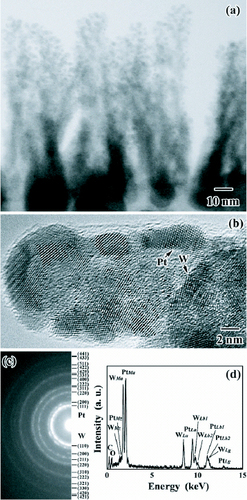
Figure 11 (a) A TEM micrograph of Pt nanodendrite structures grown on the surface of an Al2O3 substrate by EBID for 1 min with an electron fluence of 2.0×10²⁰ e cm−2; (b) the enlargement of the square area in (a) showing the nanodendrite in more detail. (Reproduced with permission from [Citation43], © 2006, Springer Science+Business Media.)
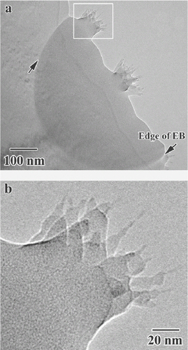
Figure 12 An HRTEM micrograph of Pt nanodendrite structures grown on the surface of an Al2O3 substrate by EBID with an electron fluence of 2.6×10²¹ e cm−2. (Reproduced with permission from [Citation43] © 2006, Springer Science+Business Media.)