Figures & data
Figure 1 XRD patterns of ITO annealed at 350 °C and deposited onto CdO buffer layers of different thicknesses.
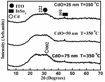
Figure 2 Transmittance spectra (200–2500 nm) for (a) as-deposited and ITO films annealed at (b) 200 °C, (c) 300 °C, and (d) 350 °C and deposited onto CdO buffer layers of different thicknesses.
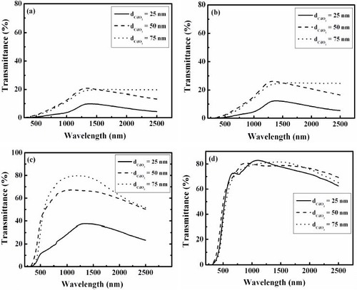
Figure 3 Plot of (αhν)2 versus hν for ITO films annealed at 350 °C and deposited onto CdO buffer layers of different thicknesses.
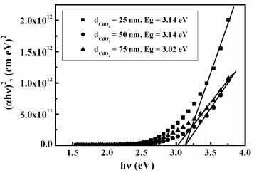
Figure 4 Extinction coefficient (k) and refractive index (n) of ITO films annealed at 350 °C and deposited onto CdO buffer layers of different thicknesses.
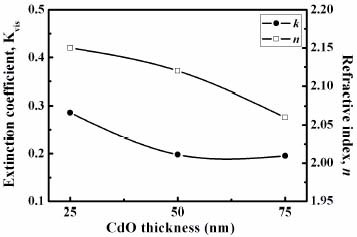
Figure 5 Dependences of packing density (p) and free carrier concentration (N) on thickness of CdO buffer layer of ITO films annealed at 350 °C.
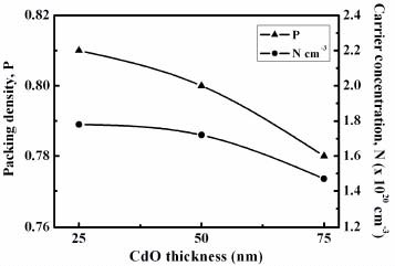
Figure 6 Plot of (a) real and (b) imaginary parts of dielectric constant as function of wavelength for ITO films annealed at 350 °C and deposited onto CdO buffer layers of different thicknesses.
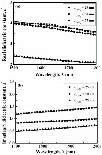
Figure 7 Annealing temperature dependence of electrical resistivity of ITO films deposited onto CdO buffer layers of different thicknesses.
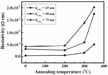
Figure 8 XRD patterns of ITO films deposited onto 25-nm-thick CdO layer heated at various temperatures.
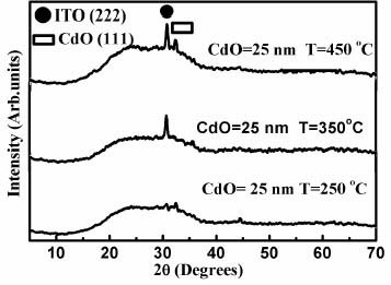
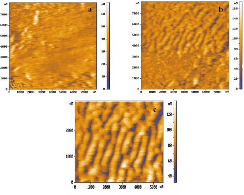
Figure 9 AFM images of ITO films deposited onto CdO-buffered glass heated at (a) 250, (b) 350 and (c) 450 °C.
Some optical properties of ITO films deposited onto 25-nm-thick CdO buffer layer heated at several temperatures.
Figure 10 (a) Transmittance and (b) reflection spectra as function of incident wavelength of ITO films deposited onto 25-nm-thick CdO buffer layers heated at various temperatures.
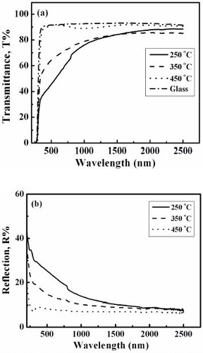
Figure 11 (a) Wavelength dependences of refractive index and (b) extinction coefficient of ITO films deposited onto 25-nm-thick CdO buffer layers heated at various temperatures.
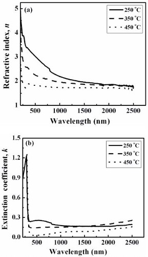
Figure 12 Variations in (a) real and (b) imaginary parts of dielectric constant with wavelength in NIR region (1700–1900 nm) of ITO films deposited onto 25-nm-thick CdO buffer layers heated at various temperatures.
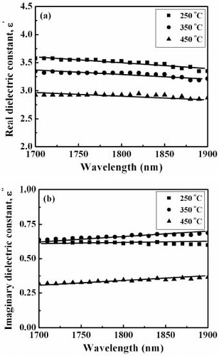
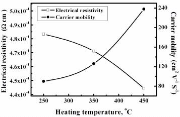
Figure 13 Variations in electrical resistivity and carrier mobility of ITO films with heating temperature of 25-nm-thick CdO buffer layers.