Figures & data
Figure 1 (a) T dependence of ρ of polycrystalline In2O3–ZnO film with weight concentration of ZnO x = 0.005 in various magnetic fields perpendicular to the film surface: H = 0, 0.1, 0.3, 1.0, 2.0, 3.0, and 4.0 T. The film was prepared by annealing as-grown amorphous In2O3–ZnO at 300 °C for 2 h. The inset shows the detailed data near the onset of superconducting transition at H=0 (•) and H = 5 T (○). (b) Normalized magnetoresistivity defined as Δ ρ = [ρ (H) - ρ (0)]/ρ (0) at temperatures T = 1.5, 2, 2.5, 3 and 3.5 K from top to bottom.
![Figure 1 (a) T dependence of ρ of polycrystalline In2O3–ZnO film with weight concentration of ZnO x = 0.005 in various magnetic fields perpendicular to the film surface: H = 0, 0.1, 0.3, 1.0, 2.0, 3.0, and 4.0 T. The film was prepared by annealing as-grown amorphous In2O3–ZnO at 300 °C for 2 h. The inset shows the detailed data near the onset of superconducting transition at H=0 (•) and H = 5 T (○). (b) Normalized magnetoresistivity defined as Δ ρ = [ρ (H) - ρ (0)]/ρ (0) at temperatures T = 1.5, 2, 2.5, 3 and 3.5 K from top to bottom.](/cms/asset/ed0f5b1c-978d-4dc2-aae1-80b7ef04d86d/tsta_a_11660803_f0001_oc.jpg)
Figure 2 (a) Cross-sectional HAADF-STEM image of grains and grain boundaries of In2O3–ZnO film with x = 0.05. (b) Intensity of HAADF–STEM and (c) EELS O-K edges. Line shows the profile taken on thick line crossing the grain boundary in HAADF–STEM image in (a). The point indicated by the arrow corresponds to the grain boundary.
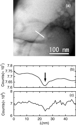
Figure 3 (a) XRD pattern of films annealed at 200 °C for different annealing times ta. (b) ta dependence of crystallinity factor P defined as P(ta) =∑Pi (ta)/∑ Pi (ta = 20 h). The quantity Pi (ta) corresponds to the peak height of diffractions (211), (222), (400), (440) and (622) for a film annealed for duration ta. (c) TEM images for films annealed at 200 °C for 0.5, 4.0 and 20 h.
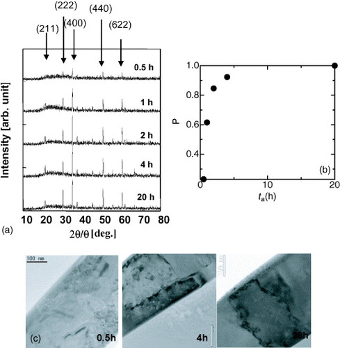
Figure 4 (a) ρ (T) dependence for films with x = 0.01 annealed at 200 °C for 0 (amorphous), 0.5, 1.0, 2.0, 4.0, 20 and 48 h from bottom to top. (b) Normalized resistance R(T)/R(T = 4.2 K) for five films annealed for 0.5, 1.0, 2.0, 4.0 and 20 h from left to right.
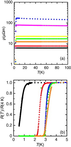
Figure 5 (a) Dependences of Tc (•) and n (▪) on annealing time ta for films with x = 0.01. The value of Tc was defined as the temperature at which half of the normal-state resistance was restored. (b) Dependence of Tc on crystallinity factor P.
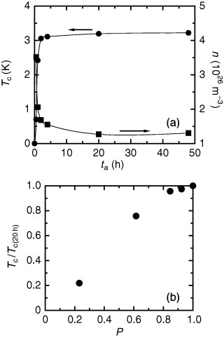
Figure 6 Dependence of Tc on carrier concentration n for films with x = 0.005 (•), x = 0.01 (▪) and x = 0.02 (▴) annealed at 200 °C. The symbols on the horizontal axis are data of as-grown amorphous films.
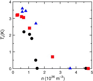
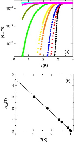
Figure 7 (a) Tdependence of ρ of In2O3–ZnO with x = 0.01 annealed at 200 °C for 2 h at magnetic fields H = 0, 0.1, 0.3, 0.8, 1.0, 2.0, 3.0, 4.0 and 6.0 T. (b) T dependence of the upper critical magnetic field Hc2.