Figures & data
Figure 1. Optical image of extrusion with streak defects
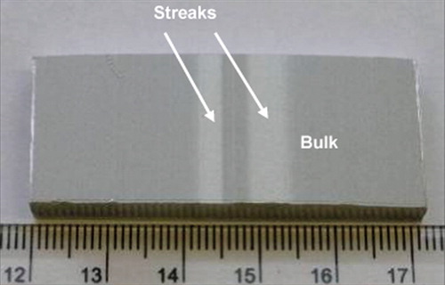
Figure 2. Total reflectance of streak (top) and bulk (bottom) regions
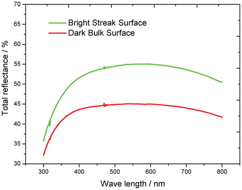
Figure 3. Optical micrographs of anodic film: polarised light was used to enhance grain orientation effect
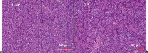
Figure 4. Backscattered electron micrographs of anodic film: insets show typical grain boundary grooves at increased magnifications
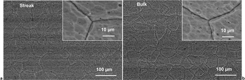
Figure 5. Backscattered electron micrographs of cross-section of anodic film attached to alloy substrate
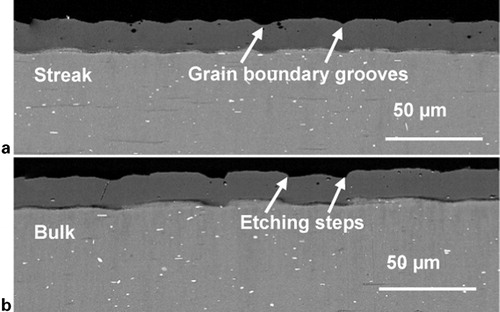
Figure 6. Map (EBSD) of alloy substrate after film stripping
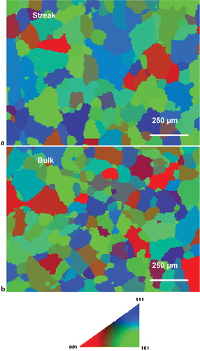
Figure 7. Optical images of alloy after a reetching and b reanodising
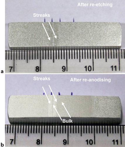
Figure 8. Optical micrographs of alloy substrate after film stripping and alkaline etching
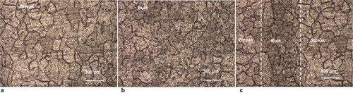
Figure 9. Interferometry topography of alkaline etched specimen
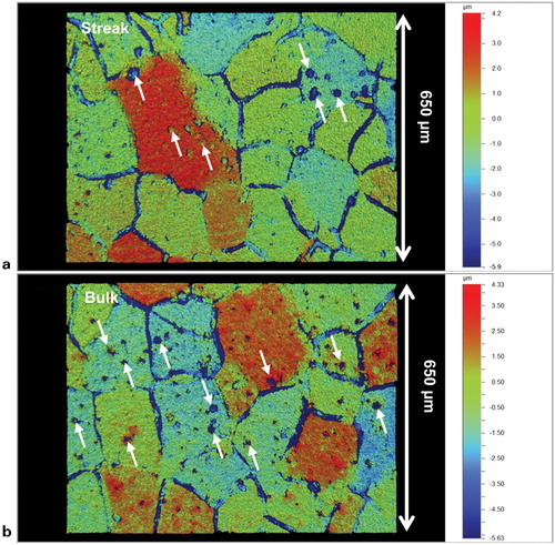
Figure 10. Images (SEM) of alloy substrate: a, b streak and c, d bulk regions. a, c are secondary electron images and b, d are corresponding backscattered electron images
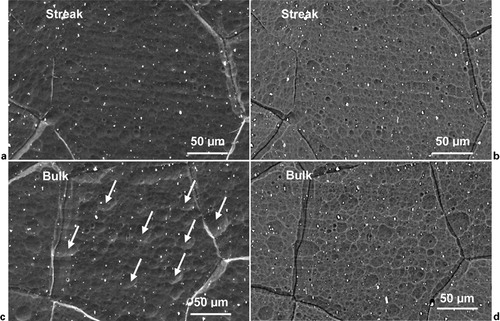
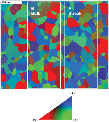
Figure 11. Map (EBSD) of as etched sample in streak/bulk interface region. Framed area A represents typical streak region and framed area B represents typical bulk region