Figures & data
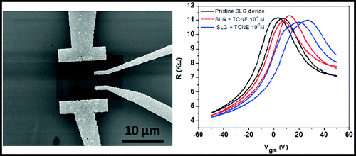
Figure 1. a Raman spectrum of a single-layer graphene (inset shows the optical image of single-layer graphene). b Atomic force microscopy (AFM) image of the single-layer graphene and c corresponding AFM height profile shows a height of ∼0.5 nm, indicating the single-layer nature of graphene sample
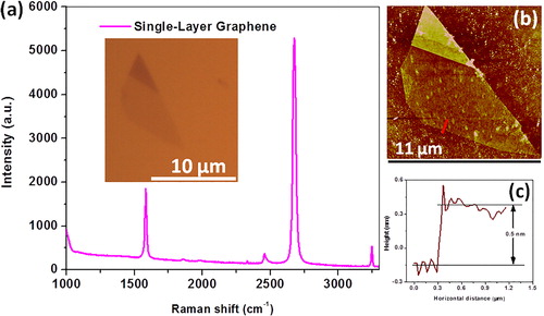
Figure 2. Typical optical images of single-layer graphene a before patterning the electrode and b after patterning the electrode. c, d Typical SEM images of the single-layer graphene field-effect transistor
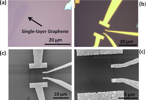
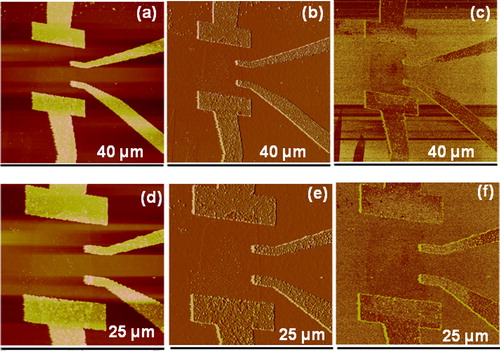
Figure 3. Typical atomic force microscopy (AFM) images of single-layer graphene field-effect transistor after annealing at a temperature of 500°C at H2 + Ar atmosphere: aand d height profile image, b and e phase image, and c and f amplitude error image
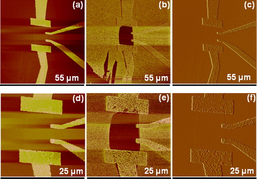
Figure 4. Typical transfer characteristics of the single-layer graphene transistor before and after TCNE decoration. The curve clearly shows the constant mobility of charge carriers in a single-layer graphene transistor with increasing chemical doping. The parallel shift indicates a negligible scattering effect of the charged impurities induced by the molecular charge–transfer doping in single-layer graphene. The curves are fast sweeps to a Vgs ± 50 V (with sweep rate of 1 V/s) from each point with Vds = 500 mV. They show that the position of the resistance peak (Dirac point) depends on the concentration of the TCNE.
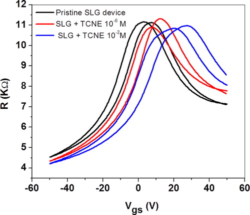
Figure 5. a Typical atomic force microscopy (AFM) image of the single-layer graphene before addition of tetracyanoethylene (TCNE), b and c are corresponding phase and amplitude error images. The AFM image of the single-layer graphene after addition of (doping) TCNE 10− 2 M concentration solution (d and g) and corresponding phase images (e and h), and amplitude error images f and i)
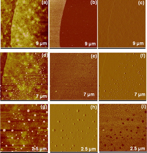
Figure 6. Atomic force microscopy (AFM) images of single-layer graphene transistor devices after addition of (doping) tetracyanoethylene (TCNE) 10− 2 M height profile images (a–d), phase images (b, e), and amplitude error images (c, f)