Figures & data
Figure 1 (A) Schematic of nano amorphous oxide semiconductor (AOS) thin film transistors (TFTs). (B) SEM of the cross section of In-Ga-ZnO(IGZO) TFTs fabricated in lab (scale bar =100 nm).
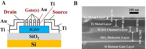
Figure 2 (A) Typical transfer curve degradation of the AOS TFTs samples under temperature stress. (B) Typical transfer curve loop of the AOS TFTs used here.
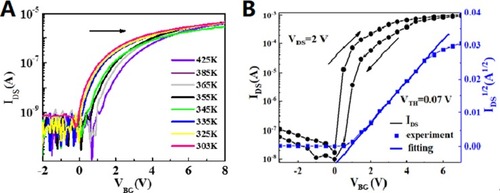
Figure 3 (A) Ultraviolet ray photoelectron spectrometer (UPS) diagram of our AOSTFTs samples before temperature stress (sample 1) and after temperature stress (sample 2). (B) Linear fitting of threshold voltage Vth as a function of temperature T.
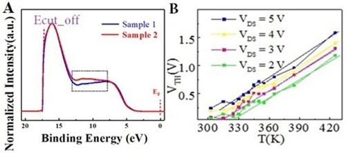
Figure 4 Transfer curves IDS vs. VGS before (in blue), under (black) and after high temperature stress (red).
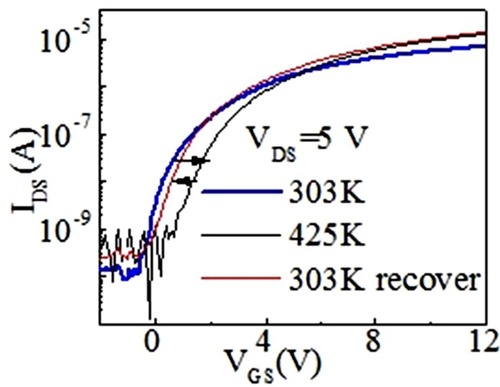
Figure 5 Temperature dependence of XPS for IGZO sample when the temperature decreases back.
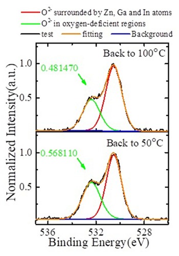
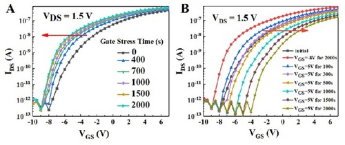
Figure 6 (A) The transfer curve with VD=1.5V under different negative gate bias stress times. (B) The transfer curve with VD=1.5V under different positive gate bias stress times.