Figures & data
Figure 1 Perspective scanning-electron microscopy images from a cross-section performed in micropatterns showing (A) alternating Si and nanostructured porous silicon stripes, (B) and Si/nanostructured porous silicon square grids. (C) Characteristic fluorescence from nanostructured porous silicon areas from a top view of a 2-D square pattern.
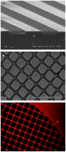
Figure 2 (A) Fluorescence microscopy images of hMSCs on 100 μm Si/25 μm nanostructured porous silicon square micropatterns. Actin is stained green and nuclei are stained blue. (B) Detailed image at an intersection, and (C) histogram of hMSC population from image (A) with absolute % and area normalized population (left and right columns respectively).
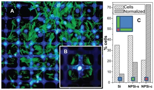
Figure 3 Adherence vector modulus for cells located on a line perpendicular to the 1-D stripe patterns for (A) 100 μm-wide Si/25 μm-wide nanostructured porous silicon (nanoPS) alternating stripes, (B) 50 μm-wide Si/25 μm-wide nanoPS stripes, (C) 35 μm-wide Si/25 μm-wide nanoPS stripes, and (D) one 2-D grid pattern of 100 μm-wide Si and 25 μm-wide nanoPS stripes. Screen capture of the program developed to perform the simulations and (E) t = 0, and (F) t = 400 seconds.
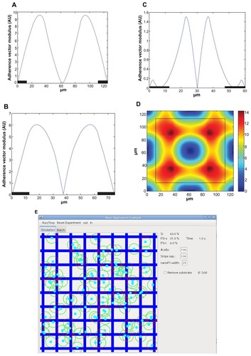
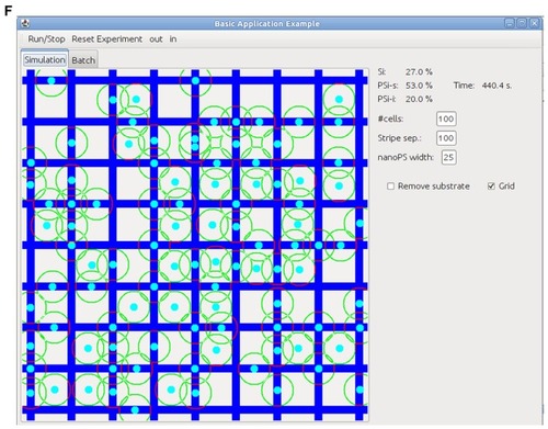
Table 1 Surface distribution of the cells for the different Si/nanostructured porous silicon micropatterns