Figures & data
Figure 1 A representative SEM micrograph of the as-grown ZnO nanostructures. The inset shows the EDS spectra of the as-grown ZnO nanostructures, which were taken for each sample to determine the content.
Abbreviations: EDS, energy disperse spectroscopy; SEM, scanning electron microscopy.
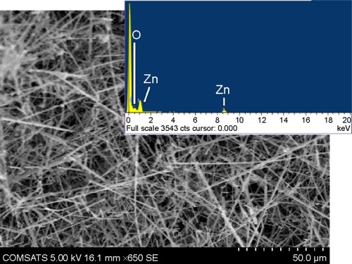
Figure 2 (A) XRD patterns of Ar-annealed ZnO nanostructures annealed in Ar at different temperatures. (B) XRD patterns of ZnO nanostructures oxidized in O2 plasma at different flow rates of oxygen.
Notes: The major peaks of ZnO are labeled. The bottom pattern in both panels is from the as-grown ZnO nanostructures.
Abbreviation: XRD, X-ray diffraction.
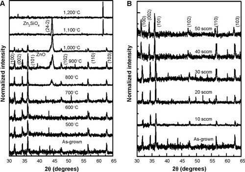
Figure 3 Magnified portion of the XRD patterns in the range from 31° to 36° for (A) Ar-annealed ZnO NS at different temperatures; (B) plasma-oxidized ZnO NS at different flow rates.
Note: A shift in (002) peak toward lower 2θ values was clearly observed in the plasma-oxidized NS.
Abbreviations: NS, nanostructure; XRD, X-ray diffraction.
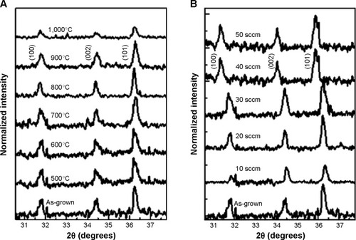
Figure 4 Plots of the variation in the (A) XRD peak positions; (B) FWHM of the (002) and (101) planes of the oxygen plasma–processed (left panel) and Ar-annealed (right panel) ZnO nanostructures; and (C) c/a values of the ZnO hexagonal crystal, as obtained from the XRD analysis.
Abbreviations: FWHM, full width at half maximum; XRD, X-ray diffraction.
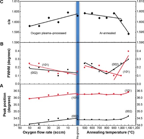
Figure 5 The variation in the atomic percentages of Zn and O in the oxygen plasma–processed (left panel) and Ar-annealed (right panel) ZnO nanostructures.
Note: At high temperature annealing, a new Zn2SiO4 phase was also observed from the XRD results.
Abbreviation: XRD, X-ray diffraction.
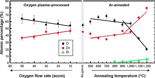
Figure 6 Schematic diagram showing the possible radiative transitions in ZnO due to various defects, such as Zn and O interstitials, and vacancies.
Notes: The diagram was used to identify the origin of various bands and peaks in the PL spectra from the postprocessed ZnO nanostructures shown in . Data from Faber et al.Citation24
Abbreviations: EC, conduction band edge; Eg, band gap energy; EV, valence band edge; IO, oxygen interstitials; IZn, Zn interstitials; PL, photoluminescence; VO, oxygen vacancies; VZn, zinc vacancies.
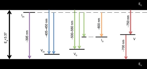
Figure 7 Room temperature photoluminescence spectroscopy of (A) Ar-annealed and (B) oxygen plasma–processed ZnO nanostructures at various annealing temperatures and oxygen flow rates, respectively.
Notes: The bottom spectra of both columns represent the PL spectra from the as-grown ZnO nanostructures. The sharp line at approxiamtely 700 nm is the Raman mode of ZnO, which was used to normalize the PL spectra. Insets show the zoomed part of NBE PL spectra of the processed ZnO NSs.
Abbreviations: PL, photoluminescence; NBE, near band edge emission; NSs, nanostructures.
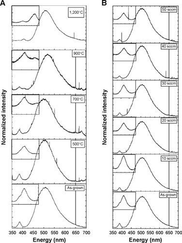
Figure 8 Variation in the (A) near band edge emissions (NBE), (B) defect assisted deep band emissions (DBE), and (C) ratio of the defect assisted deep band emissions to Near band edge emissions (DBE/NBE) of the processed ZnO NSs as a function of O2 flow rates (left panel) and annealing temperatures in Ar (right panel), respectively.
Notes: The decrease in integrated intensities of the both NBE and BDE was larger for oxidized ZnO NSs.
Abbreviations: NBE, near band edge emissions; DBE, defect assisted deep band emissions.
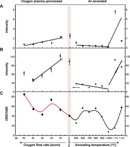
Figure 9 Optical micrographs of agar plates, showing the variation in the zone of inhibition exhibited by as-grown, Ar-annealed, and oxidized ZnO NSs. (A) and (B) for Escherichia coli while (C) and (D) for Staphylococcus aureus.
Notes: C represents the control for the ZnO powder, and P represents the kanamycin (positive control).
Abbreviation: NS, nanostructure.
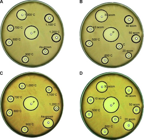
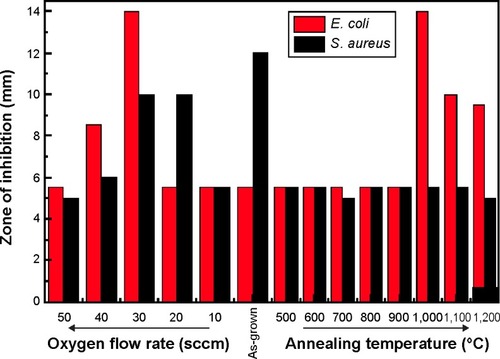
Figure 10 Bar chart of the zone of inhibition of the oxygen plasma–processed (left) and Ar-annealed (right) ZnO nanostructures against Escherichia coli (black bar) and Staphylococcus aureus (red bar).