Figures & data
Figure 1 Fabrication of silicon nanowires with top-down approach including (a) thermal oxidation, (b and c) stepper photolithography followed by bulk anisotropic etching by deep silicon reactive ion etching (DRIE), and (d) thermal oxidation with post-potassium hydroxide (KOH) solution. Their corresponding SEM images are shown in (b and d).
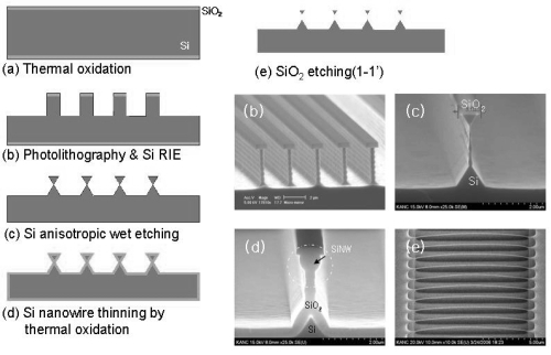
Figure 2 SiNWs transfer process for nanowire assembly (left) and their prior and post transfer (right). Free standing siNWs were transferred to photoresist layers on wafers.
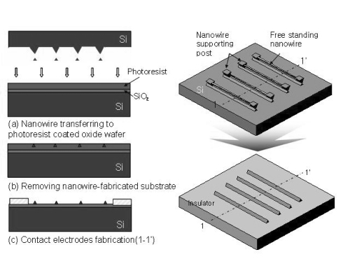
Figure 3 Electrical signal measurement system composed of (a) siNWs chip device, (b) PDMS with channel, inlet, and outlet, (c) chip with PDMS channel connected to syringe pump and outlet tube, and (d) chip-mountable probe station.
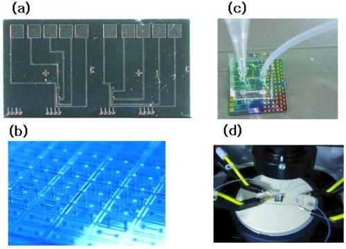
Figure 4 (a) FET characteristics of SiNW device using back-gate modulation; (b) SiNW FET device for biosensor application.
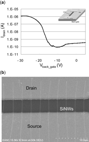
Figure 5 Schematic drawing of the process flow for passivation (left) and corresponding SEM images (right).
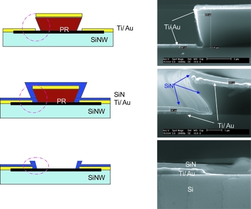
Figure 6 (a) Electrical signal change according to pH variation (pH 4 ~ 10) and (b) pH 10 to 4 at source voltage of −0.4 V with p-type siNWs. Average size of siNWs is diameter 70 nm and length 20 μm.
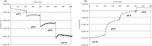
Figure 7 Graphs show experimental results from the (a) signal changes with increasing streptavidin concentration and (b) their average, and the variations of each concentration. They are mean of 4 values ± 2 SD.
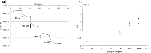
Figure 8 Real-time electrical signal measurements: (a) Signal changes with systematic delivery of 1 fM, 1 pM, and 1 nM of CRP antigen in low salt concentration (1.37 mM) and (b) signal changes from before delivery of CRP antigen. They are mean of 3 values ± 2 SD.
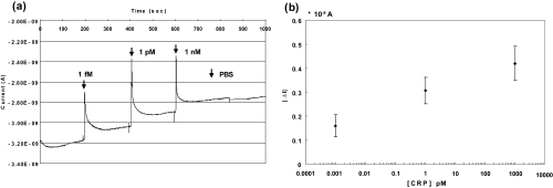
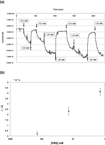
Figure 9 Real-time electrical signal measurements. Signal changes with systematic delivery of 1.37 mM, 13.7 mM, and 137 mM of PBS (left figure) and their signal changes from the base line, which corresponds to each signal at 137 mM. They are mean of 3 values ± 2 SD.