
Abstract
In this work, 750 nm-thick BaTiO3 thin films with highly (0 0 1) preferred orientation were grown on single crystal MgO substrates by RF-sputtering. Hydrogen silsesquioxane (HSQ) resist material based ridge waveguides, which were fabricated on BaTiO3 thin films, were formed by e-beam lithography. Au electrodes were deposited on top of the BaTiO3 films beside the waveguide. Propagation losses of the BaTiO3 ridge waveguide were 3–5 dB/cm in transverse electric polarization. The measured electrooptic coefficient value (r51) was 110 pm/V, which is three times larger than the electrooptic coefficient (r33 = 30.8 pm/V) of single crystal LiNbO3. SiO2 strip waveguide formed by HSQ exhibited light propagation with loss lower than 5 dB/cm. This result demonstrates potential possibility of creating highly oriented and/or epitaxially grown BaTiO3 waveguides and optical components on oxide substrates.
Keywords:
1 Introduction
Perovskite BaTiO3 materials have attracted a great deal of attention, in recent years, for its high electro-optic coefficient, as well as its piezoelectric properties, given its lead-free nature [Citation1–Citation4]. Its large electro-optic coefficient, for example, could enable the fabrication of highly miniaturized optical modulators for fiber-optic based data transmission systems [Citation5]. The electro-optic effect describes the change to the index ellipsoid due to an applied electric field. Currently, electro-optic devices are largely fabricated on bulk LiNbO3 single crystals and are combined with other optical and electronic components in hybrid form. Even with its much lower electro-optic coefficient, LiNbO3 has been the material of choice given its ability to be grown as large, high quality single crystals. Recent developments in the fabrication and characterization of thin film optical components (e.g., waveguides, sources, modulators, and detectors) suggest that integrated optical systems on silicon will soon materialize [Citation6]. Miniaturization places a premium on materials such as BaTiO3 with much higher electro-optic coefficients (e.g., r42 = 1640 pm/V compared to r42 = 20 pm/V for LiNbO3), higher data rates and/or lower operating voltages. Much progress has been achieved in recent years in the growth of high quality oxide films [Citation7,Citation8]. In particular, there has been a great deal of effort expanded in the growth of a number of ferroelectric oxides, including BaTiO3, onto Si in support of ferroelectric-based non-volatile memories [Citation9,Citation10]. By extension, the development of thin film optical modulators, capable of being integrated into a Si-based device platform, can be envisioned [Citation11]. However, several key criteria must be satisfied when integrating BT electro-optic thin films onto Si substrates. First the BaTiO3 films must be grown in an epitaxial fashion, highly oriented along the (0 0 1) direction, to optimize the electro-optic effect [Citation12–Citation14]. Second, the BaTiO3 films must be sufficiently spatially separated from the Si substrate to optically decouple the BaTiO3 based device from the lossy Si substrate. Lastly, the layers separating BaTiO3 from the underlying Si substrate should have an index of refraction lower than BaTiO3 to insure confinement of light within the waveguides and should be chemically stable in contact with both Si and BaTiO3. In this letter, we report on c-axis oriented BaTiO3 thin film electro-optic waveguide modulator fabricated on MgO, via e-beam lithography.
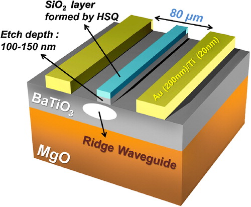
Scheme 1 Schematic diagram of SiO2 strip loaded BaTiO3 ridge waveguide structure.
2 Experimental
The BaTiO3 films were deposited on MgO(1 0 0) substrates at 550 °C by RF reactive sputtering. A disk-type BaTiO3 target of 2-in. diameter was used. The BaTiO3 films were synthesized using a fixed RF power (120 W) and an Ar/O2 (ratio 1/1) atmosphere with total pressure of 30 mTorr. Hydrogen silsesquioxane (HSQ) resist was spun onto 1 μm-thick BaTiO3 films. Ridge waveguides were patterned by e-beam lithography. The exposed HSQ is transformed into SiO2, which serves as a mask for subsequent etching of BaTiO3. The SiO2 remains as a cladding on the waveguide. The BaTiO3 films were wet chemically etched utilizing a 1:1:20 HCl:H2O2:H2O solution.
The ridge waveguide dimensions were 3 μm wide, with a ridge step height of 0.15 μm on a 1 μm thick BaTiO3 film. As a design parameter, the chip length was 6 mm and the crystal orientation of BaTiO3 was (0 0 1). 200 nm thick Au electrodes, with a 20 nm thick Ti adhesion layer, were deposited onto the BaTiO3 films with 80 μm electrode gaps. A schematic diagram of the BaTiO3 ridge waveguides is illustrated in .
3 Results and discussion
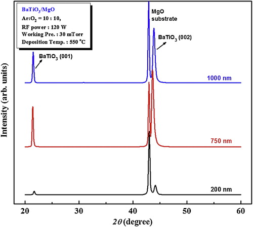
shows X-ray diffraction patterns of the BaTiO3 thin films, deposited on MgO single crystal substrates, with thicknesses ranging from 200 to 1000 nm. All BaTiO3 films showed a highly (0 0 1) preferred orientation. Discrete diffraction spots, with fourfold symmetry, were observed when a BaTiO3(1 1 0) plane was used as the diffraction plane (not shown). This result revealed that all BaTiO3 films grew epitaxially on MgO(1 0 0) substrates. Similar growth behaviors of perovskite thin films on single crystal substrates have been previously reported elsewhere [Citation15–Citation17]. A full width half maximum (FWHM) of 0.8097 for the (1 0 0) reflection of 750 nm thick BaTiO3 films points to a very well crystallized film. Compared to the 750 nm thick BaTiO3 film, the 1 μm thick BaTiO3 film showed slightly reduced crystallinity, with FWHM of 1.527. By atomic force microscopy, rms values of surface roughness of the 750 nm thick and 1 μm thick BaTiO3 films were found to be 0.863 nm and 5.16 nm, respectively. Film orientation and surface roughness are important since they impact propagation loss.
Fig. 1 X-ray diffraction pattern of BaTiO3 thin films with various thicknesses.
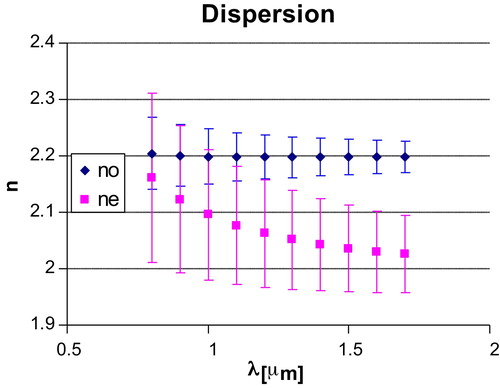
A Metricon 2010 system was used to measure the ordinary and extraordinary indices of the BaTiO3 films. The refractive indices of the transverse electric (TE) and transverse magnetic (TM) modes, measured for BaTiO3 waveguides on MgO, are listed in . The wavelength dispersion of the index of refraction is shown in . The refractive index decreases slightly as wavelength increases (normal dispersion).
Table 1 Optical properties of BaTiO3 films.
Fig. 2 Ordinary and extraordinary indices of BaTiO3 thin films as a function of wavelength.
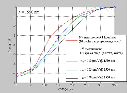
The relative transmitted optical power at 1550 nm is shown plotted in as a function of voltage for a number of voltage ramps in both increasing and decreasing directions. The effective electro-optic coefficient (r51) calculated from these measurements was 100–110 pm/V, compared with r51 of 30 pm/V for single crystal LiNbO3. Ten voltage cycles were traversed to insure reproducibility. All measurements showed similar and relatively uniform electro-optic properties.
Fig. 3 Transmitted optical power at 1550 nm as function of applied voltage demonstrating electro-optic effect in BaTiO3 thin film waveguides.
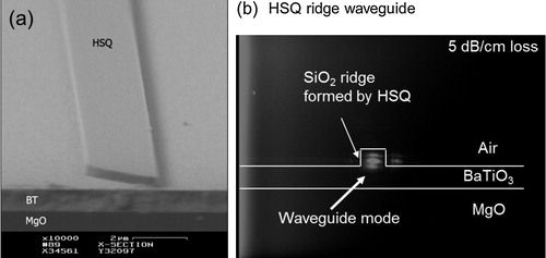
a shows SiO2 strip waveguide formed by HSQ on a BaTiO3/MgO structure and b exhibits light propagation through SiO2 strip loaded BaTiO3 ridge waveguide. Propagation loss was measured to be lower than 5 dB/cm. Light propagation was clearly observed as shown in b. We expect that further improvements in light propagation can be achieved by improving the quality of HSQ derived SiO2 by annealing.
Fig. 4 SiO2 strip loaded ridge waveguide patterned on highly oriented BaTiO3 thin films grown on MgO single crystal substrate.
4 Conclusion
In summary, highly (0 0 1) oriented BaTiO3 thin films were successfully deposited onto MgO single crystal substrates by RF sputtering. BaTiO3 ridge waveguides were formed by e-beam lithography using HSQ resist material. The propagation loss of the BaTiO3 ridge waveguide was 3–5 dB/cm in TE polarization. The measured electro-optic coefficient (r51) was approximately 110 pm/V, three times larger than the electrooptic coefficient (r33 = 30.8 pm/V) of single crystal LiNbO3. This confirms that BaTiO3 thin films with highly preferred orientation can be a promising candidate for integrated electro-optic modulators.
Acknowledgements
This work was supported, in part, by Pirelli Labs and the MIT Microphotonics Center. Thanks go to Peter Rakich for assistance with the optical measurements. This work was also supported by the Center for Integrated Smart Sensors funded by the Ministry of Education, Science and Technology as Global Frontier Project (CISS-2012M3A6A6054188).
Notes
Peer review under responsibility of The Ceramic Society of Japan and the Korean Ceramic Society.
Related Research Data
References
- M.IzdebskiW.K.UcharczykOpto-Electron. Rev.1620084245
- S.MasudaA.SekiK.ShiotaH.HaraY.MasudaJ. Appl. Phys.1092011124108
- S.CabukJ. Optoelectron. Adv. Mater.112009280288
- H.I.YooC.R.SongD.K.LeeJ. Electroceram.82002536
- B.W.WesselsAnnu. Rev. Mater. Res.372007659679
- A.LiuR.JonesL.LiaoD.Samara-RubioD.RubinO.CohenR.NicolaescuM.PanicciaNature4272004615618
- A.A.TalinS.M.SmithS.VoightJ.FinderK.EisenbeiserD.PenunuriZ.YuP.FejesT.EschrichJ.CurlessD.ConveyA.HooperAppl. Phys. Lett.81200210621064
- I.D.KimY.AvrahamiH.L.TullerY.B.ParkM.J.DickenH.A.AtwaterAppl. Phys. Lett.862005192907
- Y.DreznerM.NitzaniS.BergerAppl. Phys. Lett.862005042906
- S.Y.YangB.T.LiuJ.OuyangV.NagarajanV.N.KulkarniR.RameshJ.KidderR.DroopadK.EisenbeiserJ. Electroceram.1420053744
- C.DubourdieuI.GelardO.SalicioG.Saint-GironsB.VilquinG.HollingerInt. J. Nanotechnol.72010320347
- J.HiltunenD.SeneviratneR.SunM.StolfiH.L.TullerJ.LappalainenV.LanttoJ. Electroceram.222009416420
- S.KumariA.KhareIEEE J. Quantum Electron.48201210361039
- S.BernhardtL.MizeP.DelayeG.RoosenJ. Appl. Phys.92200261396148
- J.HeH.Q.JiangJ.C.JiangE.I.MeletisJ. Mater. Sci.47201227632769
- T.HosokuraK.KageyamaH.TakagiY.SakabeJ. Am. Ceram. Soc.932010630633
- J.HiltunenD.SeneviratneH.L.TullerJ.LappalainenV.LanttoJ. Electroceram.222009395404