
 ?Mathematical formulae have been encoded as MathML and are displayed in this HTML version using MathJax in order to improve their display. Uncheck the box to turn MathJax off. This feature requires Javascript. Click on a formula to zoom.
Abstract
Transparent conducting Tin doped Cadmium oxide thin films were prepared by sol–gel spin coating method with different Sn concentrations. X-ray diffraction analysis reveals the polycrystalline nature of the Cadmium oxide (CdO) with cubic structure and show preferential orientation along (111) plane. The surface morphology of prepared films was analyzed by SEM and surface roughness variations analyzed by water contact angle measurement. The EDX spectra confirmed the presence of Cd, Sn and O elements in the films. The blue shift of energy gap from 2.42 to 2.96 eV is explained by Burstein–Moss effect. The presents of functional groups and the chemical bonding are confirmed by FTIR spectra. The minimum electrical resistivity (1.12 × 10⁻⁴ Ω cm) and maximum carrier concentration (9.94 × 1021 cm−3) was obtained for 5% of Sn doped CdO thin film.
| Nomenclature | ||
| β | = | full width at half maximum (rad) |
| D | = | crystallite size (nm) |
| λ | = | wavelength of X-ray (Å) |
| θ | = | Bragg’s angle (°) |
| d | = | lattice spacing (Å) |
| ɛ | = | micro-strain |
| h, k, l | = | Miller indices |
| α | = | absorption coefficient |
| T | = | transmittance (%) |
| hν | = | photon energy (eV) |
| Eg | = | optical band gap (eV) |
| ρ | = | resistivity (Ω cm) |
| n | = | carrier concentrations (cm−3) |
| μ | = | mobility (cm/Vs) |
1 Introduction
The transparent conducting oxide (TCO) such as Indium oxide, Tin oxide, Zinc oxide and Cadmium oxide have wide applications in the field of optoelectronic devices. Among these TCO's the Cadmium oxide (CdO) have been successfully used for many applications such as gas sensor, photovoltaic photo diodes and transparent electrodes, etc…, due to its low resistivity, high carrier concentration and high optical transmittance in the visible region of solar spectrum [Citation1,Citation2]. The CdO is has acute toxicity (oral, dermal and inhalation) but we use this material due to its unique properties and applications. A variety of techniques were reported for CdO thin film deposition, including pulsed laser deposition [Citation3], metal–organic chemical vapor deposition (MOCVD) [Citation4], spray pyrolysis [Citation5], successive ionic layer adsorption and reaction (SILAR) method [Citation6], chemical bath deposition [Citation1], RF magnetron sputtering [Citation7] and sol–gel process [Citation8]. Among these methods the sol–gel spin coating process has several advantages such as simplicity, composition control and homogeneity. CdO is a n-type semiconductor with band gap in the range of 2.2–2.8 eV [Citation9]. Many researchers studied the optoelectronic properties of CdO doping with different metallic ions Indium [Citation10], Aluminum [Citation11], Gallium [Citation12] and Manganese [Citation13]. The effect of Tin doping on the physical properties of CdO thin films has already been reported by a few researchers. Zheng et al. [Citation3] studied the effect of Sn doping on structural, optical and electrical properties of CdO thin films by pulsed laser deposition. They observed the band gap was increased and electrical resistivity was decreased as increasing Sn concentration. Sahin et al. [Citation6] reported that the SILAR prepared CdO films show a band gap was increased from 2.09 to 2.39 eV with increasing Sn concentration. Gupta et al. [Citation14] reported temperature dependence of Sn doped CdO thin films by pulsed laser deposition method. Sn4+ ion has four valence electrons (5s2, 5p2) and the ionic radius of Sn4+ ion (0.69 Å) is slightly smaller than that of Cd2+ ions (0.95 Å), thus we expect that Sn4+ ions doping in CdO will lead to improvement in electrical conductivity by increasing electron concentrations [Citation15]. In this paper, we are reporting the effect of Tin (Sn) doping on structural, surface, optical and electrical properties of Cadmium oxide (CdO) thin films by sol–gel spin coating method.
2 Experimental
The films were deposited on borosilicate glass substrates by sol–gel spin coating method. First the Cadmium acetate di-hydrate (Merck 99.0%) was dissolved in methanol (Merck 99.9%) (0.2 M) at a constant magnetic stirring and then acetic acid (Merck 99.8%) (0.2 M) was added to the stirring solution as a stabilizer. For Sn doping the Tin (II) chloride di-hydrate (Merck 98.0%) was dissolved in the above solution with different percents (0, 1, 3 and 5 wt%). The Tin (II) chloride is easily soluble in ethanol and it is a suitable material for sol–gel process. The final solution was stirred for 1 h at 80 °C to yield a clear and homogeneous solution. The final solution was used as the coating source after cooling down to room temperature. The coating solution was dropped into the cleaned glass substrates (1 sq.in.) fixed at the top base of the spin coating unit, which was rotated at 3000 rpm for 30 s. After the coating all the films were dried at 150 °C for 10 min to evaporate the solvent. To obtain the desired film thickness, this procedure was repeated for five times and finally the resulting thin films were annealed at 450 °C in the air for 1 h.
The structure of the prepared films was characterized by X-ray diffractometer (PANalytical) with Cu Kα1. The scanning electron microscopy (ESEMQUANTA200, FEI-Netherland) were performed to analyze the surface morphology of the films. Elemental analysis was made by energy dispersive X-ray spectroscopy (attached to SEM). The variations of surface roughness were analyzed by micro photographs (FUJIFILM FinPix S3300) and the contact angle measured using a protractor. The film thickness was measured by a profilometer (SJ-301Mitutoyo). The optical transmittance of the films was recorded using UV–vis spectrophotometer (Oceans optics HR2000-USA). The presence of chemical bonding was studied by FTIR spectrophotometer (Perkin Elmer – RXI). The electrical properties were measured using a Hall-effect setup.
3 Results and discussion
3.1 Structural properties
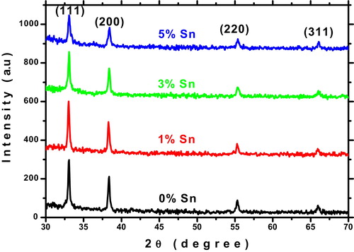
The X-ray diffraction patterns of un-doped and Sn doped CdO thin films are given in . The peaks in the XRD pattern of the prepared films were appearing at (111), (200), (220), and (311) directions without any impurity and secondary phases. The observed diffraction patterns indicate the polycrystalline nature of the CdO with a cubic structure (JCPDS card No: 75-0592). As seen in the intensity of the all peaks is decreased and broadened with Sn doping concentration indicates shrinkage of crystallite size. Similar phenomenon had been reported already for Sn doped CdO thin films [Citation3,Citation6].
Fig. 1 XRD patterns of prepared thin films for different Sn doping concentrations.
The crystalline size of the films was estimated using Debye Scherrer's formulae [Citation9],(1)
(1) And the dislocation density (δ) and strain (ɛ) were calculated using the following relations [Citation9],
(2)
(2)
(3)
(3) where λ (1.54060 Å) is the X-ray wavelength, θ is Bragg's angle and β is full width at half maximum (FWHM). The obtained crystallite size is decreased as the increasing doping concentration which related to strain. The calculated inter planer distance and lattice constant values for (111) direction was good agreement with JCPDS file data (75-0592). The slight changes of inter planer distance and lattice constants may due to the substitution of smaller ionic radii Sn4+ (0.69 Å for 6 co-ordination number) instead of larger ionic radii Cd2+ (0.95 Å) in the crystal lattice [Citation15]. The dislocation density (δ) and strain (ɛ) were calculated for all the films from the diffraction data to obtain more information about structural properties and it is presented in . The observed changes of strain are due to the point defects and crystallite size [Citation16].
Table 1 Structural parameters of CdO thin films for different Sn concentrations.
3.2 Surface morphology and compositional analysis
The surface morphology was analyzed for all films deposited with different Sn concentrations. shows the scanning electron microscopic (SEM) images (unit scale is 1 μm) and micro photographs of un-doped and Sn doped CdO thin films. It is observed that the Sn doped CdO thin films have uniform and homogeneous coverage of spherical grains. The size of the grains and voids slightly decreased with increasing Sn doping level, which may due to intrinsic stress caused by incorporation of foreign atoms. The surface morphology of Sn doped CdO films is more uniform than reported results by SILAR method [Citation6].
Fig. 2 Scanning electron microscope (SEM) images and microphotograph of water droplet on surface of prepared thin films.
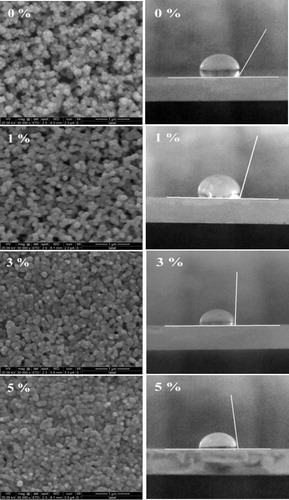
The micro photographs show water droplet on the prepared substrates to measure the water contact angle. The observed contact angle (∼118°, 103°, 93° and 84° for 0%, 1%, 3% and 5%, respectively) is decreased as increasing Sn doping level indicates the reduction of surface roughness [Citation17]. The rough surface may diffuse the incident light, hence reduce the optical transmittance [Citation18].
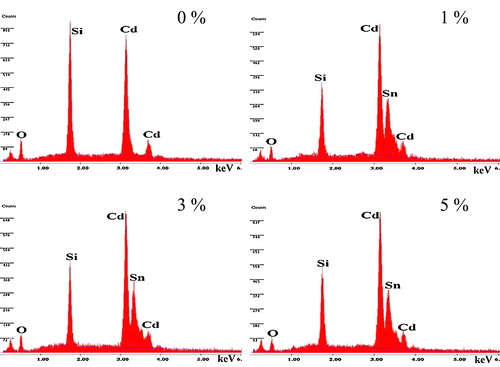
Energy dispersive X-ray spectroscopy (EDX) is an analytical technique used for the chemical characterization of a sample. shows the EDX spectra of the prepared films. The spectrum reveals that the presence of Cd, O and Sn elements in the deposited films. The weight percentage is almost equal to their nominal stoichiometry within the experimental error as shown in . The Silicon (Si) signal appears to originate from the glass substrates.
Table 2 The quantitative analysis of elements present in thin films using EDX spectrum.
Fig. 3 EDX spectra of the undoped and Sn doped CdO thin films.
3.3 Optical properties
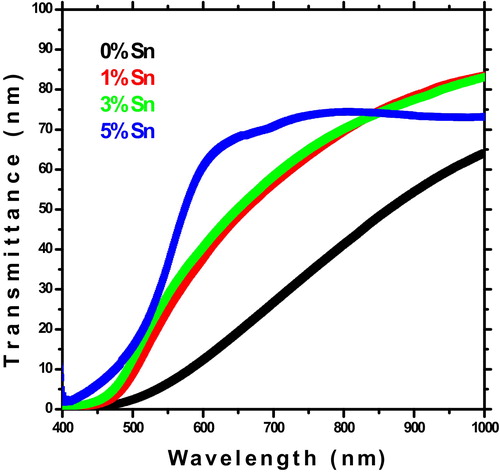
The optical transmittance spectra of Sn doped CdO thin films with different doping concentration are shown in . It can be observed that the average transmittance of the un-doped CdO films lies in the range of 45–50% in the visible region. For Sn doped CdO films the average transmittance has improved to 72%. This value is higher than reported values for Sn doped CdO films by SILAR method [Citation6]. From the figure it is clear that the transmittance of CdO films improved as Sn doping level. This effect of CdO films may be due to the reduction of surface roughness as shown in micro photographs of water contact angle. On the other hand, there is a shift of the absorption edge into lower wavelengths as Sn doping level. Similar results were observed for Aluminum doped CdO thin films prepared by the spray pyrolysis method [Citation5].
Fig. 4 UV–vis transmittance spectra of undoped and Sn doped CdO films.
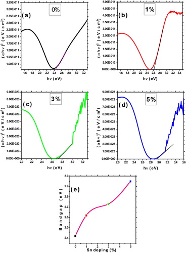
The optical band gap of Sn doped CdO thin films was estimated by extrapolation of the linear portion of the (αhν)2 versus hν plots. The absorption coefficient (α) is calculated using the following equation [Citation19],(5)
(5) where T is transmittance and d is film thickness. The absorption coefficient (α) and the incident photon energy (hν) is related by the Tauc's relation as follows [Citation20],
(6)
(6) where hν, A, and Eg are photon energy, constant and optical band gap respectively. (a–d) shows the plots of (αhν)2 versus photon energy (hν) for Sn doped CdO film. The calculated band gap values plotted as a function of Sn doping concentration is shown in (e). From the figure the band gap value of the pure CdO film is 2.42 eV, which gradually increases up to 2.96 eV for 5 wt% of Sn doping. This value is higher than reported value of Sn doped CdO thin films by pulsed laser deposition (2.93 eV) [Citation3], SILAR (2.39 eV) [Citation6] and chemical bath deposition (2.84 eV) [Citation20]. Also higher than other TCO materials such as CdO:Al (2.8 eV) [Citation21] CdO:F (2.88 eV) [Citation22] CdO:In (2.72 eV) [Citation23]. Higher band gaps are required for any optoelectronic application, particularly for solar cell applications. The blue-shift of energy band gap appeared due to electrons populated states within the conduction band which pushes the Fermi level to higher energy and related to the Burstein–Moss effect [Citation24].
Fig. 5 The plots of (αhν)2 versus hν; (a) 0%, (b) 1%, (c) 3% and (d) 5%. (e) Optical band gap (Eg) as a function of Sn concentrations.
3.4 FTIR analysis
The Fourier transform infrared (FTIR) spectroscopy is the most common technique to identify the chemical bond structure. The FTIR spectrum diagram of the Sn doped CdO films is shown in . The broad absorption peak at around 3400–3600 cm−1 is attributed to normal polymeric O–H stretching vibration of H2O in CdO lattice. The peaks at 800–1400 cm−1 is assigned to CdO [Citation25]. The bands in the region of 520–670 cm−1 can be ascribed to the stretching vibration of Sn–O [Citation26]. An upward shift (527.84–551.03 cm−1) in the frequency of the present system is due to the presence of Sn in Cd–O lattice.
Fig. 6 FTIR spectra of CdO thin films for different Sn concentrations.

3.5 Electrical properties
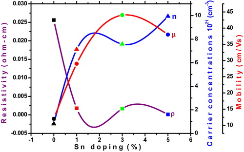
illustrates the variation in resistivity (ρ), carrier concentrations (n), and Hall mobility (μ) as a function of Sn concentration in CdO thin films. It can be seen that the electrical parameters were strongly influenced by Sn doping in the CdO films. As the Sn concentration increases from 0 to 5 wt%, the resistivity decreases from 2.56 × 10⁻² Ω cm to the minimum value of 1.12 × 10⁻⁴ Ω cm. The obtained resistivity value (1.12 × 10⁻⁴ Ω cm) is lower than Sn doped CdO thin films prepared by pulsed laser deposition method (1.59 × 10⁻⁴ Ω cm) [Citation3] chemical bath deposition (8 × 10⁻⁴ Ω cm) [Citation21] and metal organic chemical vapor deposition (3.1 × 10⁻⁴ Ω cm) [Citation27]. The un-doped CdO thin film exhibit a carrier concentration of 0.81 × 1021 cm−3. This is improved with Sn doping level and obtained a maximum of 9.94 × 1021 cm−3 for 5 wt%. The improvement of carrier concentration may originate from the replacement of Cd2+ ions by Sn4+ ions in the CdO lattice. The maximum mobility 44 cm2/Vs were obtained for 3 wt%. As is well known, resistivity is proportional to the reciprocal of the product of carrier concentration and mobility. The reduction of electrical resistivity may due to reduction of voids and improved carrier concentration. The electrical conductivity and mobility is more sensitive for grain interface than defects of crystals.
Fig. 7 Resistivity (ρ), carrier concentration (n) and mobility (μ) of the CdO thin films as a function of Sn concentrations.
4 Conclusions
The following are the conclusions drawn from the present investigation:
| • | Sn doped CdO thin films were prepared by sol–gel spin coating method on glass substrate. The effects of Sn concentration on structural, surface, optical and electrical properties of CdO thin films were investigated as a function of the Sn doping concentration. | ||||
| • | The XRD analysis revealed good crystallinity of cubic structure with preferred (111) crystal orientation in the films. The crystallite size of the prepared films decreased as increasing Sn doping concentrations. | ||||
| • | SEM images show that the Sn doped CdO thin films have a uniform surface with spherical grain. The water contact angle measurements indicate the reduction of surface roughness. EDX spectra confirmed the presence of Cd, Sn and O elements with nominal stoichiometry. | ||||
| • | The optical band gap of the films is increasing with increasing Sn content and approaching a maximum value of 2.96 eV for 5 wt%. | ||||
| • | The presents of functional groups and chemical bonding were confirmed by FTIR analysis. | ||||
| • | The Sn doping in CdO films effectively increases the carrier concentration and reduces its resistivity. A maximum carrier concentration of 9.94 × 1021 cm−3 with a minimum resistivity of 1.12 × 10⁻⁴ Ω cm achieved when the film is doped with 5 wt% of Sn. | ||||
Thus the sol–gel spin coating is a good technique for producing nano-structured materials. Sn doped CdO is a good candidate for optoelectronic devices based on the tunable band gap and high conductivity.
Notes
Peer review under responsibility of The Ceramic Society of Japan and the Korean Ceramic Society.
References
- R.R.SalunkheV.R.ShindeC.D.LokhandeSens. Actuators B: Chem.1332008296301
- F.YakuphanogluAppl. Surf. Sci.257201014131419
- B.J.ZhengJ.S.LianL.ZhaoQ.JiangVacuum852011861865
- D.A.LampS.J.C.IrvineJ. Cryst. Growth33220111720
- R.KumaravelS.MenakaS.Regina Mary SnegaK.RamamoorthiK.JeganathanMater. Chem. Phys.1222010444448
- B.SahinT.TaskopruF.BayansalCeram. Int.40201487098714
- B.SahaS.DasK.K.ChattopadhyaySol. Energy Mater. Sol. Cells91200716921697
- F.YakuphanogluSol. Energy85201127042709
- M.Azizar RahmanM.K.R.KhanMater. Sci. Semicond. Process.2420142633
- R.K.GuptaK.GhoseR.PatelS.R.MishraP.K.KaholMater. Lett.62200833733375
- I.S.YahiaG.F.SalemM.S.Abd El-sadekF.YakuphanogluSuperlattices Microstruct.642013178184
- R.J.DeokateS.V.SalunkheG.L.AgawaneB.S.PawarS.M.PawarK.Y.RajpureA.V.MoholkarJ.M.KimJ. Alloys Compd.4962010357363
- K.SankarasubramanianP.SoundararajanT.LoguS.KiruthigaK.SethuramanR.Ramesh babuK.RamamurthiMater. Sci. Semicond. Process.262014346353
- R.K.GuptaK.GhoshR.PatelS.R.MishraP.K.KaholMater. Lett.62200841034105
- R.D.ShannonActa Crystallogr.A321976751767
- V.D.MoteY.PurushothamB.N.DoleJ. Theor. Appl. Phys.62012613
- M.ThirumoorthiJ.Thomas Joseph PrakashSuperlattices Microstruct.852015237247
- M.J.KimH.T.KimJ.K.KangD.H.KimD.H.LeeS.H.LeeS.H.SohnMol. Cryst. Liq. Cryst.53220102128
- R.K.GuptaK.GhoshR.PatelS.R.MishraP.K.KahoCurr. Appl. Phys.92009673677
- L.R.de León-GutiérrezJ.J.Cayente-RomeroJ.M.Peza-TapiaE.Barrera-CalvaJ.C.Martínez -FloresM.Ortega-LópezMater. Lett.60200638663870
- K.SirajM.Khaleeq-ur-RahmanS.I.HussainM.S.RafiqueS.AnjumJ. Alloys Compd.509201167566762
- M.KulM.ZorA.S.AybekS.IrmakE.TuranSol. Energy Mater. Sol. Cells912007882887
- R.KumaravelK.RamamurthiV.KrishnakumarJ. Phys. Chem. Solids71201015451549
- E.BursteinPhys. Rev.931954632701
- A.TadjarodiM.ImaniMater. Lett.65201110251027
- L.CaoL.HuoG.PingD.WangG.ZengS.XiThin Solid Films3471999258262
- Z.Y.ZhaoD.L.MorelC.S.FerekidesThin Solid Films4132002203211