
 ?Mathematical formulae have been encoded as MathML and are displayed in this HTML version using MathJax in order to improve their display. Uncheck the box to turn MathJax off. This feature requires Javascript. Click on a formula to zoom.
Abstract
Indium tin oxide (ITO) thin films have been prepared by jet nebulizer spray pyrolysis technique for different Sn concentrations on glass substrates. X-ray diffraction patterns reveal that all the films are polycrystalline of cubic structure with preferentially oriented along (222) plane. SEM images show that films exhibit uniform surface morphology with well-defined spherical particles. The EDX spectrum confirms the presence of In, Sn and O elements in prepared films. AFM result indicates that the surface roughness of the films is reduced as Sn doping. The optical transmittance of ITO thin films is improved from 77% to 87% in visible region and optical band gap is increased from 3.59 to 4.07 eV. Photoluminescence spectra show mainly three emissions peaks (UV, blue and green) and a shift observed in UV emission peak. The presence of functional groups and chemical bonding was analyzed by FTIR. Hall effect measurements show prepared films having n-type conductivity with low resistivity (3.9 × 10⁻⁴ Ω-cm) and high carrier concentrations (6.1 × 1020 cm−3).
| Nomenclature | ||
| D | = | Crystallite size (nm) |
| k | = | Scherrer’s constant |
| d | = | Lattice spacing (Å) |
| h,k,l | = | Miller indices |
| TC | = | Texture coefficient |
| I(hkl) | = | Peak intensity |
| N | = | Number of peaks |
| T | = | Transmittance (%) |
| hν | = | Photon energy (eV) |
| Eg | = | Optical band gap (eV) |
| n | = | Carrier concentrations (cm−3) |
| β | = | Full width at half maximum (rad) |
| λ | = | Wavelength of X-ray (Å) |
| θ | = | Bragg’s angle (deg) |
| ɛ | = | Strain |
| α | = | Absorption coefficient |
| ρ | = | Resistivity (Ω-cm) |
| μ | = | Mobility (cm/(V s)) |
1 Introduction
Indium tin oxide (ITO) is a well known n-type transparent conducting oxide material. Here tin acts as a cationic dopant in the In2O3 lattice and as a substitute on the indium sites to bind with the interstitial oxygen. Due to its high optical transmittance, electrical conductivity and wide band gap (>3.5 eV), ITO has been widely applied in various optoelectronic devices such as photovoltaic cells [Citation1], liquid crystal displays [Citation2] and gas sensors [Citation3]. The ITO thin films are commonly fabricated by employing different techniques such as magnetron sputtering [Citation4–Citation8], sol–gel process [Citation9–Citation11], thermal evaporation [Citation12], pulsed laser deposition [Citation13,Citation14], chemical vapor deposition [Citation15,Citation16], spray pyrolysis [Citation17–Citation22] and nebulizer spray pyrolysis (NSP) [Citation23]. All of these methods have advantages and disadvantages, but jet nebulizer spray pyrolysis has a noticeable advantage; it is a low-cost and non-vacuum technique for large area applications and can produce high quality film with low precursor volume. The working of NSP method is based on the Bernoulli principle; i.e., when a pressurized flow of air is directed through a constricted orifice, the velocity of the airflow is increased to create a jet stream. The impact of a jet stream with liquid produces aerosol particles (particle size ∼2.5 μm) [Citation24]. The mist form of solution is helping to improve the quality of film and to obtain a uniform growth due to gradual nucleation with minimum wastage. In the present study, the tin doped indium oxide thin films were prepared by a simple and low-cost jet nebulizer spray pyrolysis technique. The structure, surfaces, optical, photoluminescence and electrical properties of prepared films were investigated in detail.
2 Experiment
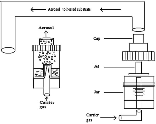
A jet nebulizer spray pyrolysis apparatus () is used in this work, which consists of a jet nebulizer spraying unit, substrate holder with heater and air compressor. To prepare tin doped indium oxide thin films, the indium (III) chloride (InCl3) is dissolved in 100 mL double distilled water to make 0.4 M starting solution. Tin doping was achieved by adding tin (II) chloride dihydrates (SnCl2·2H2O) to the starting solution. A few drops of acetic acid were added to obtain a clear and homogeneous solution. The doping level in the solution was varied from 0 to 30 wt% in steps of 10 wt%. The mixture was stirred under constant speed for 1 h with a magnetic stirrer. Prior to the deposition, glass substrates (1 in.2) were cleaned with acetone, isopropyl alcohol, and distilled water successively for 15 min in ultrasonicator. The substrate temperature for each deposition was kept at 500 °C in the air atmosphere. The prepared solution was sprayed with a jet nebulizer (HUDSON RCI micro mist, droplet size is ∼2.7 μm) on the heated substrate with spray rate 0.5 mL/min using compressed air as a carrier gas. The nebulizer was kept at a distance of 5 cm from substrate surface.
Fig. 1 Schematic diagram of jet nebulizer apparatus.
The structural parameters of spray coated ITO films were analyzed by X-ray diffractometer (XRD) using the PANalytical system with Cu Kα1 radiation (k = 1.54056 Å). Surface morphology and topography were carried out by the scanning electron microscope (ESEMQUANTA200, FEI-Netherlands) and atomic force microscopy (Agilent 5500) respectively. Elemental analysis was made by using energy dispersive X-ray spectroscopy (attached to SEM). The water contact angle measurement was made by using a protractor from microphotograph. The optical properties of the films were examined with a double beam spectrophotometer (Oceans optics HR2000-USA) in the UV–vis regions. The film thickness was measured by a profilometer (SJ-301 Mitutoyo). The photoluminescence (PL) spectra were recorded using a spectrofluorometer (Cary Eclipse EL08083851) with xenon arc lamp. The IR spectrum was recorded using FTIR spectrophotometer (Perkin Elmer – RX I) in the range of 400–4000 cm−1. The electrical parameters were collected from room temperature Hall effect measurements (RH2035 PhysTech GmbH) system.
3 Results and discussion
3.1 Structural analysis
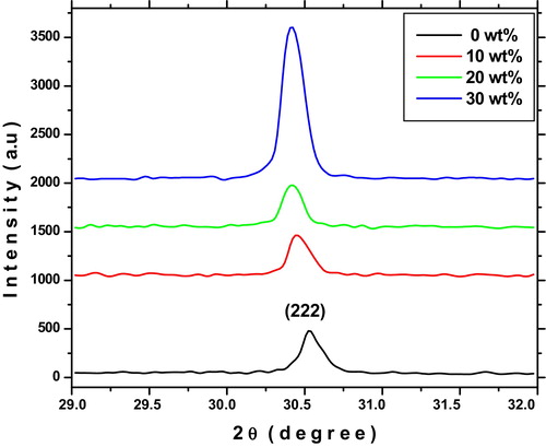
X-ray diffraction patterns are used to study the crystal structure of prepared ITO thin films. shows the X-ray diffraction patterns of indium tin oxide thin films for different tin concentrations on glass substrates. It can be seen that all the films are polycrystalline in nature and crystallize in a cubic structure (JCPDS: 71-2194) with predominant (222) peak. A switching in the preferential growth from the (400) to (222) planes was observed when tin doped with indium oxide. The increasing intensity of the (222) plane is attributed to the increase in the degree of preferential crystal orientation. It is evident from the XRD spectra that no diffraction peaks of Sn or other impurity phases are detected in the prepared samples. As shown in shift of the (222) peak toward smaller 2θ value is due to the replacement of smaller radius Sn4+ ion (0.71 Å) in indium sites and also related to changes of strain in the crystal lattice [Citation25].
Fig. 2 X-ray diffraction patterns of ITO thin films for different Sn concentrations.
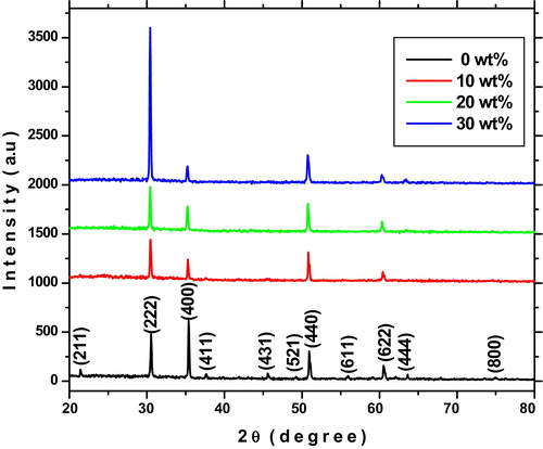
Fig. 3 Shift of peak position of ITO thin films along (222) plane for different Sn concentrations.
The crystallite size was calculated from the XRD pattern using Debye-Scherrer formula [Citation26]:(1)
(1) where λ is X-ray wavelength (λ = 1.54060 Å), β is full width at half maximum in radian and θ is Bragg’s angle.
The dislocation density (δ) and strain (ɛ) were calculated using the following equations [Citation26]:(2)
(2)
(3)
(3)
Texture coefficient (TC) measures the relative degree of preferred orientation among crystal planes, which is obtained from following expression [Citation27]:(4)
(4) where I(hkl) is the measured intensity of the plane (hkl), Io (hkl) is the standard intensity of the respective diffraction plane, according to the JCPDS data card (71-2194) and N is the number of diffraction peaks presented.
The calculated structural parameters of prepared ITO thin films using the above equations are listed in . The observed improvement in average crystallite size is attributed to strain formed in the nano crystal. The dislocation density (δ) is to measure the disorder of lattice planes in the crystal structure. The strain arises due to point defects (vacancies, site disorder), dislocations and extended defects in the crystal structures. The calculated values of the lattice constant ‘a’ are in good agreement with standard values (71-2194). Obtained lattice constant values are slightly increased for (222) plane with increased doping level, which can be related to uniform-strain of the grains. The texture coefficient TC (hkl) values calculated for the different planes of the films are shown in . The results indicate that the preferential orientation for pure indium oxide film along (400) plane, is shifted to (222) plane for Sn doped indium oxide films. The change of preferred orientation may be due to occupancy of additional indium vacancy sites by tin atoms which are unoccupied previously. In fact, it is well known that In2O3 thin films have several defect levels such as indium interstitial oxygen and indium vacancies [Citation28]. The increase in preferred orientation is associated with the increase of crystallite growth along that plane. The change in peak intensity, d-value, lattice constants and strain confirms the substitution of Sn into In–O lattice.
Table 1 Structural parameters of prepared ITO thin films for different Sn concentrations.
3.2 Surface morphological analysis
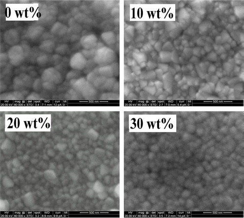
For thin films the surface morphology depends on the deposition technique and its parameters. The surface morphology may influence the film properties such as mechanical, electrical and optical properties. shows the scanning electron microscopic images of ITO films for different Sn concentrations deposited on glass substrates. It can be seen that all the films have a uniform surface morphology consisting of spherical particles without any voids and cracks. The lowering grain boundary and large active surface help to improve the electrical conductivity and optical transmittance.
Fig. 4 Scanning electron microscopy images (60,000× magnification) of prepared ITO thin films.
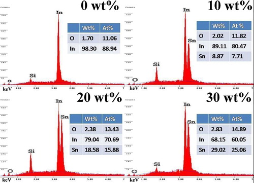
Energy dispersive X-ray spectroscopy (EDX) is an analytical technique used for the elemental analysis of a sample. The EDX spectra of the prepared ITO thin films are shown in . The spectra reveal that the presence of In, O and Sn elements in the deposited films. The weight percentage is almost nearly equal to their nominal stoichiometry within the experimental error.
Fig. 5 Energy dispersive X-ray spectra of ITO thin films.
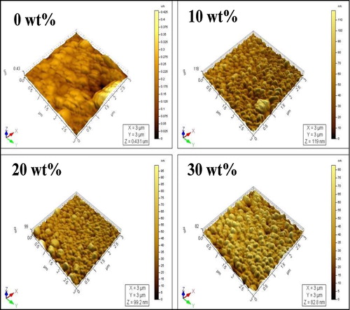
Topography is one of the most important physical characteristics of surfaces, which influence their significant technical properties. shows the 3D-AFM images of prepared ITO thin films for different Sn concentrations. The un-doped indium oxide film has a large difference between peak and valley than Sn doped films. As shown in the surface profile parameters are changed with increasing Sn concentration. The surface roughness (Sa) and root mean square (RMS) (Sq) values are reduced as increasing Sn concentrations. The obtained RMS value of ITO films is lower than the prepared one by other techniques such as ink-jet printing [Citation29], RF sputtering [Citation30], chemical vapor deposition [Citation31] and spray pyrolysis [Citation32]. The average roughness is the mean value of peak and valley as calculated over the measured entire surface area. It is useful for detecting general variations in overall profile height characteristics. Root mean square roughness is the square root of the distribution of surface height and is considered to be more sensitive than the average roughness. It represents the standard deviation of the profile heights and is used in the computations of skewness and kurtosis. Surface skewness (Ssk) is used to measure the symmetry of the variations of surface about the mean line and is more sensitive to occasional deep valleys or high peaks. Surface kurtosis (Sku) is used to measure the distribution of the spikes above and below the mean line. The roughness reduction of the films helps to reduce the scattering of incident light and leading to increase of optical transmittance.
Table 2 Height parameters of ITO thin film obtained from AFM analysis.
Fig. 6 AFM 3D images of prepared ITO thin films for different Sn concentrations.
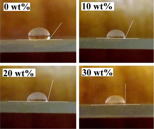
shows the microphotographs of water droplet on the ITO surface, and thus it can be perceived that the water contact angles (127°, 114°, 106° and 92° for 0, 10, 20 and 30 wt% respectively) are decreased. This result indicates that the hydrophilicities of ITO surface are increased with Sn doping concentrations, and such a behavior is due to reduction of surface roughness.
Fig. 7 Microphotographs of water droplet on ITO surface.
3.3 Optical studies
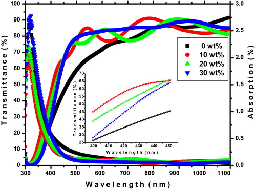
The optical properties of thin films are known to depend strongly on the film thickness, microstructures, levels of impurities and deposition parameters. shows the optical transmittance and the absorption spectrum of prepared ITO thin films for different doping concentrations. It is found that the average transmittance of the pure indium oxide film is 77% and that of the Sn doped films could be in the range of 82–87%, and such results may be related to low scattering of light and thickness. As shown in (inset) the absorption edge is shifted to lower wavelength for Sn doped indium oxide films. The transmission spectra show just the opposite trend of the optical absorption spectra. The absorption of all the films is in the range of 0.04–1.10% in the visible region, the low absorption of incident light is essential for TCO.
Fig. 8 UV–vis transmittance and absorption spectrum of ITO thin films. Inserted image shows the blue shift of absorption edges.
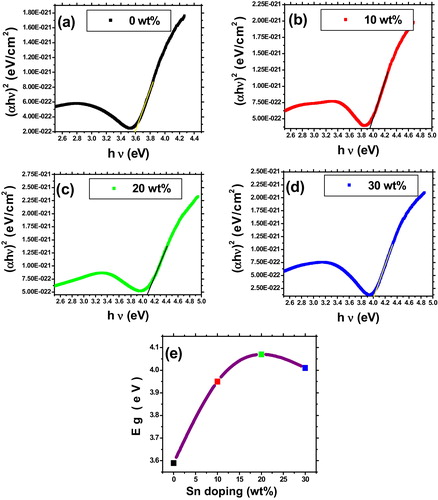
The optical band gap (Eg) values calculated from the plot of (αhν)2 versus (hν) is shown in (a)–(d) for the prepared films. The absorption coefficient (α) is calculated from the following relation [Citation26]:(5)
(5) where d is thickness of the films and T is transmittance. The absorption coefficient (α) and incident photon energy (hν) is related by the following relation [Citation26]:
(6)
(6) where A is a constant, hν is photon energy and Eg is optical band gap. Obtained band gaps are plotted as a function of Sn concentrations that are shown in (e). It is observed that band gap increases rapidly from 3.59 eV (0 wt%) to 4.07 eV (10 wt%) and then decreased slightly to 4.01 eV (30 wt%). Similar behavior of band gap widening and then narrowing for higher doping of tin is reported previously by Benamar et al. [Citation20]. The widening of the optical band gap is related to increased carrier concentration and which is explained by using Moss–Burstein effect [Citation33]. The narrowing of band gap for higher Sn doping may be due to many-body interaction effects either between free carriers or between free carriers and ionized impurities [Citation34].
Fig. 9 (a–d) The (αhν)2 versus hν plots of ITO thin films for different Sn concentrations; (e) variations of optical band gap as function of Sn concentrations.
3.4 Photoluminescence studies
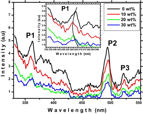
The room temperature photoluminescence (PL) spectroscopy technique is a selective and extremely sensitive probe of discrete electronic states. shows the room temperature PL spectra of ITO thin films recorded under the excitation wavelength λ = 310 nm. Mainly three emission peaks are observed as follows: a strong UV emission peak (P1 at 363 nm), a strong blue emission peak (P2 at 493 nm) and a weak green emission peak (P3 at 521 nm). The UV emission peak is also called near band edge (NBE) emission, and it originates due to the recombination of the free exciton through an exciton–exciton collision process [Citation35]. As shown in (inset) a change observed in the UV emissions peak indicated that the recombination centers are modified by Sn doping. A blue emission band indicated that a new defect level is introduced into the band gap by the Sn doping [Citation36]. The origin of green emission is generally ascribed to deep level defects such as surface defects and singly ionized oxygen vacancies [Citation37]. A rapid decrease in the intensity of all peaks and the change of UV emission peak position confirm the substitution of Sn atom in indium sites.
Fig. 10 Room temperature photoluminescence (PL) spectrum of ITO thin films; (insert) the observed change of UV emissions peaks position.
3.5 FTIR analysis
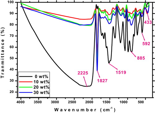
FTIR technique is used to obtain information about the chemical bonding and the presence of certain functional groups in a material. shows the FTIR spectra of prepared ITO thin films for different Sn concentrations. The broad band around 3500–1900 cm−1 is attributed to the O–H stretching vibrations of hydroxyls from absorbing water molecules [Citation38]. We can also recognize the strong absorption band at 1827 cm−1 is related to C=O stretching vibration of carboxylic acids, a medium band at 1519 cm−1 is related to C=C stretching vibration of arenes and a medium band at 885 cm−1 is ascribed to C–H bending vibration. The weak bands at 592 cm−1 and 433 cm−1 are attributed to In–O bond [Citation39].
Fig. 11 FTIR spectra of ITO thin films for different Sn concentrations in wave number range from 400 to 4000 cm−1 at room temperature.
3.6 Electrical studies
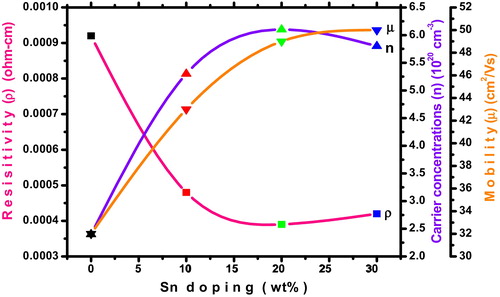
shows the measured electrical parameters of prepared ITO thin films as a function of different Sn concentrations. It can be seen that the resistivity is decreased, carrier concentration is increased and mobility is increased as increasing Sn concentrations, and this behavior is desirable for transparent conducting oxide. The results indicate that the prepared ITO thin films are highly degenerating n-type conductivity. The increase of carrier concentration value of ITO film is due to the valence difference between Sn4+ and In3+ ions, which generates extra one free carrier per atomic substitution and leading to decrease of resistivity. The incorporation of Sn dopant in indium oxide films changes the overall electrical properties significantly. We obtained a minimum electrical resistivity (3.9 × 10⁻⁴ Ω-cm) and maximum carrier concentration (6.1 × 1020 cm−3) for 20 wt% of tin doped indium oxide thin film. Similar results were reported in previous literature by Seki et al. [Citation40]. The increase of mobility is related to reduction of grain boundary scattering. The electronic transport property for the ultrathin films is entirely related to the microstructure of the films and doping concentration.
Fig. 12 Electrical parameters of prepared ITO thin films as function of Sn concentrations.
4 Conclusions
Transparent conducting indium tin oxide (ITO) thin films were successfully prepared by jet nebulizer spray pyrolysis technique. Effects of Sn doping concentrations on structure, surface, optical, photoluminescence and electrical properties were investigated. The following conclusions are derived after these investigations:
| • | The XRD patterns revealed that prepared ITO films are polycrystalline in nature with cubic structure. We observed a shift of preferential growth from (400) plane for pure indium oxide to (222) plane for Sn doped indium oxide thin films. The change observed in the peak position of (222) plane and structural parameters confirms the substitutions of Sn in In–O lattice. | ||||
| • | SEM images show the uniform distribution of spherical particles and the surface morphology also changed with Sn doping. | ||||
| • | The EDX spectrum reveals the presence of In, O and Sn elements in the deposited films with their nominal percentage. | ||||
| • | According to the 3D-AFM images the surface topography of the films is better than undoped films. The roughness and root mean square values are reduced as increased Sn concentrations. | ||||
| • | Optical transmissions of the films have improved from 77% to 87% and show an opposite trend of the optical absorption results. The observed initial blue shift in energy band gap from 3.59 to 4.07 eV can be explained by the Burstein–Moss effect. | ||||
| • | The decreasing photoluminescence peak intensity and observed shift in UV emissions peak positions is indicating the substitution of Sn in In–O system. | ||||
| • | The presence of functional groups and chemical bonding was confirmed by FTIR. | ||||
| • | Hall effect measurements show that Sn doping in indium oxide films effectively increases the carrier concentration and reduces its resistivity with an improvement in the mobility. | ||||
From these findings, we conclude that ITO thin films are suitable for optoelectronic applications and the jet nebulizer spray pyrolysis technique is suitable for producing uniform thin films with good quality.
Notes
Peer review under responsibility of The Ceramic Society of Japan and the Korean Ceramic Society.
References
- B.G.LewisD.C.PaineMRS Bull.2520002227
- J.C.ManifacierThin Solid Films901982297307
- G.NeriA.BonavitaG.MicaliG.RizzoE.CalloneG.CarturanSens. Actuators B1322008224233
- J.H.ParkC.BuurmaS.SivananthanR.KodamaW.GaoT.A.GessertAppl. Surf. Sci.3072014388392
- K.-S.TsengY.-L.LoAppl. Surf. Sci.285P2013157166
- K.C.HeoY.k.SohnJ.S.GwagCeram. Int.412015617621
- Y.S.JungD.W.LeeD.Y.JeonAppl. Surf. Sci.2212004136142
- A.Klo EppelW.KriegseisB.K.MeyerA.ScharmannC.DaubeJ.StollenwerkJ.TrubeThin Solid Films3652000139146
- Y.WangJ.LiuX.WuB.YangAppl. Surf. Sci.3082014341346
- M.T.KesimC.DurucanThin Solid Films54520135663
- L.KorosiS.KorosiI.DekanyThin Solid Films519201131133118
- K.-Y.PanL.-D.LinL.-W.ChangH.C.ShihAppl. Surf. Sci.27320131218
- J.B.ChoiJ.H.KimK.A.JeonS.Y.LeeMater. Sci. Eng. B1022003376379
- J.M.DekkersG.RijndersD.H.A.BlankAppl. Phys. Lett.882006151908
- Y.C.ParkY.S.KimH.K.SeoS.G.AnsariH.S.ShinSurf. Coat. Technol.16120026269
- Y.S.KimY.C.ParkS.G.AnsariB.S.LeeH.S.ShinThin Solid Films4262003124131
- V.BrinzariI.DamaskinL.TrakhtenbergB.K.ChoG.KorotcenkovThin Solid Films5522014225231
- P.K.ManojB.JosephV.K.VaidyanD.Sumangala Devi AmmaCeram. Int.332007273278
- H.El RhalebE.BenamarM.RamiJ.P.RogerA.HakamA.EnnaouiAppl. Surf. Sci.2012002138145
- E.BenamarM.RamiC.MessaoudiD.SayahA.EnnaouiSol. Energy Mater. Sol. Cells561999125139
- A.R.BabarS.S.ShindeA.V.MoholkarC.H.BhosaleJ.H.KimK.Y.RajpureJ. Alloys Compd.509201131083115
- K.RavichandranK.ThirumuruganJ. Mater. Sci. Technol.302201497102
- S.MarikkannuM.KashifN.SethupathyV.S.VidhyaS.PiramanA.AyeshamariamM.BououdinaN.M.AhmedM.JayachandranMater. Sci. Semicond. Process.272014562568
- V.GowthamiM.MeenakshiP.PerumalR.SivakumaC.SanjeevirajaMater. Sci. Semicond. Process.27201410421049
- G.B.GonzalezJ.B.CohenJ.H.HwangT.O.MasonJ.P.HodgesJ.D.JorgensenJ. Appl. Phys.89200125502555
- M.ThirumoorthiJ.Thomas Joseph PrakashSuperlattices Microstruct.852015237247
- S.S.ShindeP.S.ShindeS.M.PawarA.V.MoholkarC.H.BhosaleK.Y.RajpureSolid State Sci.10200812091214
- Y.-R.LyuT.-E.HsiehSurf. Coat. Technol.2312013219223
- H.-Y.LaiT.-H.ChenC.-H.ChenMater. Lett.65201133363339
- T.KonryR.S.MarksThin Solid Films4922005313321
- N.WolfM.RydzekD.GerstenlauerM.Arduini-SchusterJ.ManaraThin Solid Films53220136065
- E.S.RajK.L.ChoyMater. Chem. Phys.822003489492
- E.BursteinPhys. Rev.931954632701
- A.WalshJ.L.F.Da SilvaS.-H.WeiPhys. Rev. B782008075211
- A.UmarB.KarunagaranE.K.SuhY.B.HahnNanotechnology17200640724079
- Y.A.CaoW.S.YangW.F.ZhangG.Z.LiuP.L.YueNew J. Chem.282004218222
- Y.LiY.BandoD.GolbergAdv. Mater.152003581585
- R.J.KellerThe Sigma Library of FTIR Spectravol. 21986Sigma ChemicalSt. Louis
- R.A.NyquistR.O.KagelInfrared Spectra of Inorganic Compoundsvol. 41971Academic PressNew York
- S.SekiY.SawadaM.OgawaM.YamamotoY.KagotaA.ShidaM.IdeSurf. Coat. Technol.169–1702003525527