
1 Introduction
Current material research is exploring new strategies by tailoring the properties of the dielectric ceramic materials. Dramatic alteration can be done on the most of the properties of micro crystalline ceramics by reducing the size to nano scale. Nano crystalline oxide ceramic is the key functional material for many advanced applications. With reduction in size, the structural features of the matter lies between bulk material and that of isolated atom giving rise to number of interesting properties due to increased surface to volume ratio, which is to be surface and quantum confinement effects. Niobium oxide materials can be used as structural materials in a wide range of uses covering advanced engineering applications such as aircraft and automotive technologies as well as electronics, computation and material sciences.
Reports are available on the preparation of RETiNbO6 by the solid-state ceramic route [Citation1,Citation2], microwave hydrothermal method [Citation3,Citation4]. The orthorhombic ternary oxides of the type RE(AB)O6 [A = Ti, Hf; B = Ta, Nb] has been studied by several investigators [Citation5 Citation2013;Citation12]. RETiNbO6 is reported as a useful material for electric resonator applications [Citation13]. However, most of these methods involve high temperature annealing with intermediate grindings in order to obtain an appreciable phase purity which yields large coarse-grained micron sized powders. Combustion technique is capable of producing nano-crystalline powders of oxide material, at a lower calcination temperature in a surprisingly short time. In this paper, we report for the first time the synthesis of phase pure nano-particles of RETiNbO6 (RE = Dy, Er, Gd and Yb) without any calcination by a modified combustion technique.
2 Experimental
RETiNbO6 (RE = Dy, Er, Gd and Yb) (hereby abbreviated as DTN, ETN, GTN, YbTN, respectively) is prepared by modified combustion technique using the corresponding metal nitrate as oxidizing agent and suitable fuel as reducing agent [Citation14]. Calculations are based on the principles used in propellant chemistry, keeping fuel to oxidant ratio unity in order to produce maximum energy [Citation15]. In this synthesis, high-purity niobium pentachloride (NbCl5, 99.9%), titanium isopropoxide (Ti[OCH(CH3)2]4, 98%) and the respective rare earth oxides are used as cation sources (oxidizing agent), and urea (NH2CONH2) is used as fuel (reducing agent). Dhak et al. [Citation16] used Nb2O5 in tartaric acid solution after heating in hot water bath for 10 h to prepare niobium based ceramic. NbCl5 dissolved in oxalic acid solution without any heat treatment. Citric acid is used as complexing agent to get precursor complex [Citation17]. Stoichiometric amount of oxidizing agents and reducing agents are dissolved in a minimum volume of deionized water to obtain transparent aqueous solutions in a glass beaker and it is heated using a hot plate at 250 °C in a ventilated fume hood to get a viscous gel. The gel thus formed undergoes dehydration on further heating and self-ignites with the evolution of huge quantity of gases. Hence the residual ash that is formed after combustion has a fluffy nature. This ash is further heated up to 600 °C to get the pure phase nano powder of the samples.
3 Characterization
The XRD (Model: Philips PW1710 diffractometer) is used to determine the formation of the desired phase, for the powder. The crystallite size is calculated from X-ray line broadening by the Scherrer equation:(1) where, D is the crystal size in nm, λ is the CuKα1 wavelength (1.5406 Å), β is the halfwidth of the peak in rad, and θ is the corresponding diffraction angle.
The particle size of the prepared powders is also analyzed by the TEM (Model: TM-300, Philips). The sample is prepared by sonicating a pinch of the sample for half an hour using acetone as dispersing solvent and then is taken on a carbon coated (50 nm thickness) copper grid of 300 mesh.
The Fourier Transform infrared (FTIR) spectra of the samples are recorded in the range 400–4000 cm−1 on a Thermo-Nicolet Avatar 370 Fourier Transform Infrared Spectrometer by KBr pellet method. The Fourier Transform-Raman spectrum of the as prepared samples are carried out at room temperature in the wavenumber range 50–1200 cm−1 using Bruker RFS/100S Spectrometer at a power level of 150 mW and at a resolution of 4 cm−1. The prepared powder is mixed with one drop of 1 wt% solution of polyvinyl alcohol and uniaxially pressed at room temperature for 1 min at the pressure 190 MPa. The sintering of the pressed pellet is done with the help of furnace. The density of the sintered pellet is measured. The microstructures of the sintered sample is analyzed by SEM (Mode: JEOL JSM-5800) taken on the polished surfaces. The polished surface is coated with gold by sputtering before taking the micrograph. The dielectric constant, conductance and the tangent loss (tan δ) measurements are done at radio frequency range on the polished pellet samples as a function of frequency (100 kHz) using an LCR metre (HIOKI, model 3532, Japan). The electrical parameters are measured using an impedance analyzer (HIOKI LCR HI Tester, Model: 3532) as a function of temperature over a wide range of frequencies (100 Hz–5 MHz) after drying the silver coated sample. Optical absorbance of the samples is recorded at room temperature using a Cary 100 Bio UV–vis spectrophotometer in the wavelength range from 200 nm to 900 nm. The photoluminescence spectra of the samples are measured using a Flurolog@-3 spectrofluorometer. The photons from the source are filtered by an excitation spectrometer. The monochromatic radiation is then allowed to fall on the disc samples, and the resulting radiation is filtered by an emission spectrometer and then fed into a photomultiplier detector. The variation of intensity is recorded as a function of wavelength
4 Results and discussion
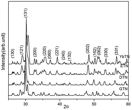
shows the XRD patterns of DTN, ETN, GTN, YbTN nano powders. This indicates that all powders crystallize in orthorhombic euxenite structure with space group pbcn in excellent agreement with the respective ICDD files 27-0205, 20-1216, 27-0221, 20-1434 and 14-0643. The diffraction peaks are broad and no secondary phase is detected. The broad peaks indicate the presence of particle of very small crystalline size [Citation18]. The crystallite size calculated from full-width-half-maximum (FWHM) using Scherrer formula for the major (131) peak is around 19 nm for GTN, 22 nm for DTN, 23 nm for ETN, and 22 nm for YbTN nano powders [Citation19]. The XRD result indicates that the formation of RETiNbO6 phase is complete during the combustion process itself without the need for any calcination unlike in the case of conventional solid state route reported elsewhere [Citation13].
Fig. 1 XRD pattern of as-synthesized powder samples.
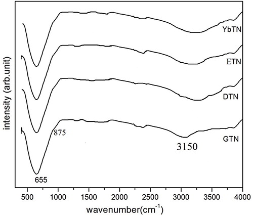
The FT-IR spectra are characterized by appearance of several deeps in the curve corresponds to the vibrational bands in the compounds in transmittance mode of measurement. The composition and quality of the product are analyzed by the FT-IR spectra shown in . The bands are assigned on the basis of Nb/TiO6 octahedral. All the compounds show identical vibration of IR active asymmetric stretching mode of Nb/TiO6 octahedra is observed strong absorption band at 655 cm−1. The shoulder peak at 875 cm−1 is due to Raman active symmetric stretching mode of TiO6 octahedra [Citation20]. The band around 3150 cm−1 is characterized as water molecules (O–H stretching modes in crystallization water). No appreciable change in bands corresponds to the characteristic Nb/TiO6 octahedra have been observed as the substitution of rare earth-site in the compound.
Fig. 2 FT IR spectra of the as-synthesized samples.
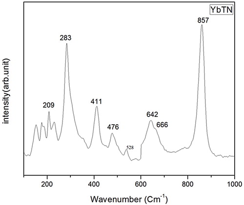
Choosing YbTN as a representative sample, Raman spectrum is taken and is shown in . The symmetric and asymmetric stretching vibration of Nb-O/Ti-O bonds give rise to two Raman active modes υ1A1g and υ2Eg modes, respectively. υ1A1g mode observed at 857 cm−1 and υ2Eg at 642 cm−1 with a shoulder band at 666 cm−1. υ3F1u is active in 528 cm−1 as very weak band. υ4F1u due to bending vibrations of Nb–O/Ti–O octahedral is observed as medium intense band at 476 cm−1. The symmetric bending vibration gives rise to υ5F2g at 411 cm−1. The band at 283 cm−1is the active mode υ6F2u and that below 200 cm−1 is due to lattice vibrations [Citation21 Citation2013;Citation23].
Fig. 3 FT Raman spectrum of the sample YbTN.
TEM analysis of samples provided further insight into the structural properties of as synthesized powders. (a–d) shows the TEM images of the samples of DTN, ETN, GTN, YbTN nano powders and the morphology is clearly observed. The diameters of the crystals are 23 nm for GTN, 28 nm DTN, 24 nm for ETN and 21 nm for YbTN.
Fig. 4 (a–d) TEM images of as-synthesized powders of GTN, DTN, ETN, YbTN nano powders.

Most of the applications require sintered products having desired shape, size and microstructure. Thus the sintering behaviour of samples synthesized through the combustion method is studied. The samples are sintered to highly dense pellets (>94% of the theoretical density) at relatively low temperature around 1250 °C only for 2 h. This shows that the samples are highly sinteractive. Some benefits associated with this preparation method regarding sintering is low sintering temperature, fast densification, small grain size end product, elimination of sintering aids, and less expensive sintering equipment. Grain boundaries play a vital role in ceramic processing. When temperature increases the grain boundary merging and grain growth will take place. In RETiNbO6 (RE = Dy, Er, Gd, Yb) nano-particles system the grain growth enhances for c-axis direction. Therefore rods like grains are observed in the sample shown in . The grains are well separated by the grain boundaries. Similar SEM images are obtained for niobate compounds [Citation24].
Fig. 5 (a) and (b) shows the SEM micrographs of the samples DTN and YbTN.

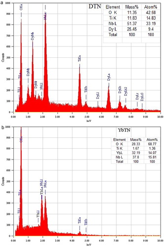
(a) and (b) shows the SEM micrographs of the samples DTN and YbTN respectively, indicating the shrinkage behaviour. Clean and elongated grains are observed microstructures of material with minimum porosity and uniform grain size are developed with sintering. The grains and grain boundaries are well defined and clearly visible. The microstructure is overall dense, but a few scattered pores are observed which indicates that there is a certain degree of porosity in the sample. The average grain size lies between 1 to 3 μm. The EDS spectra of DTN and YbTN samples are given in (a) and (b), respectively. These spectra show that all the constituent elements are present in the samples in the same stoichiometric concentrations.
Fig. 6 (a) and (b) EDS spectra of DTN and YbTN samples.
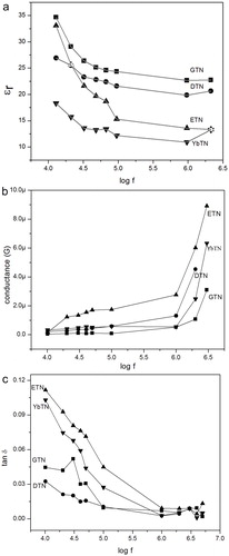
The variation of the dielectric constant (εr), AC conductance (G) and loss factor (tan δ) with radio frequency range are obtained for the sintered sample. Dielectric constant decreases initially with the increase in frequency and it reached a constant value at higher frequency range shown in (a). This is due to Maxwell–Wagner interfacial polarization [Citation25]. The decrease in dielectric constant is due to the delay in polarization with the application of the electric field because of inertia. When frequency increases, those with large relaxation time cease respond and results the decrease of dielectric constant. And at low frequency range the variation of AC conductance is very less and almost constant up to 1 MHz, and then increases according to the increase in frequency shown in (b). Thus this material can be useful for capacitive applications in communication systems.
The variation of tan δ in RF region is shown in (c). Loss reached a minimum value and almost constant as frequency increases in accordance with Koops phenomenological model [Citation26]. It means that, material has low loss in RF because of the relaxation frequency of the sample is out of this frequency range. Therefore, dissipation of electrical energy is low at this range. The studies of the variation of AC conductance, dielectric loss and dielectric constant, cleared that the materials can be effectively useful for communication applications.
Fig. 7 Variation of (a) dielectric constant (b) conductance & (c) loss factor with frequency.
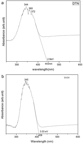
Absorption spectra of the samples DTN and YbTN are measured in the range from 200–600 nm is given in (a–b). These absorption spectra clears that the samples absorbs heavily with in UV region and moderately in visible region. That means the as prepared nano-materials are respond to the UV radiation. The optical absorption in the wavelength region shorter than 400 nm is due to the electron transition from the top of the valence band to the bottom of the conduction band [Citation27]. Such materials are useful for filter and UV sensor application. From UV–vis absorption spectra band gaps calculated for DTN and YbTN are 2.8 eV and 3.03 eV, respectively. NbO6 octahedra in as prepared samples showed a lowering of symmetry at lower preparation temperature. The decrease in band gap with respect to the conventional sample can be attributed to the presence of oxygen vacancies [Citation28].
Fig. 8 (a–b) Absorption spectra of DTN and YbTN.
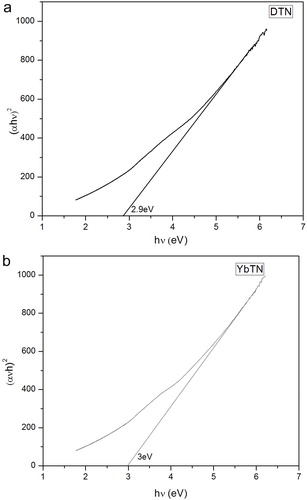
This absorption dependence on photon energy is expressed by the Tauc’s equation. According to the Tauc’s relation the absorption coefficient, for direct band gap material is given bywhere, B is an energy independent constant, α is the absorption coefficient, Eg is the optical band gap energy, h is the Planck’s constant, ν is the frequency of incident photon and m is an index which depends on the nature of electronic transition responsible for the optical absorption. Values of m for allowed direct and non-direct transitions are 1/2 and 2, respectively. Optical transitions of materials are indirect one. The indirect optical energy gap can be obtained from the intercept of the resulting linear region with the energy axis at (αhν)2 = 0 [Citation29]. (a–b) shows the Tauc’s plot of the optical absorption spectrum measured at room temperature for the samples. Thus determined band gap of DTN and YbTN are 2.9 eV and 3 eV, respectively, which is approximately equal to what we got from the absorption spectra itself.
Fig. 9 (a–b) shows the Tauc’s plot of DTN and YbTN.
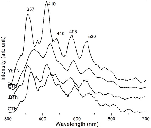
The PL emission spectra of all samples with excitation wavelength 270 nm at room temperature are given in . The spectra show maxima in the violet region and a minimal peak in the blue–green region of the visible region. Vidya et al. have reported that the completely disordered structure is suitable for a good PL emission in the red region and a complete ordered structure is suitable for a good PL emission in the green region. This indicates that the structure of the samples formed by the combustion method is completely ordered, which is evidently confirmed by vibrational analysis [Citation30]. The transitions of the constituent elements of compounds causing emissions are identified on the basis of the data by Payling and Larkins [Citation31]. The sample showed good luminescent property in the visible region. The broad peak at 530 nm is attributed to 4P1.5–4F02.5 transition of niobium. The transition 3F4 –1G°4 of titanium is the reason for emission at 410 nm. The peak at 458 nm corresponding to the transition 4F2.5–4F02.5, 2D2.5–4S01.5, 4P 2.5–4D02.5 can be assigned to rare earth elements [Citation28,Citation32]. The other weak peaks are due to the presence of oxygen vacancies present in the as prepared sample. Thus the samples are very useful for optoelectronic applications such as lasers, optical amplifiers, etc. because of their strong emission intensity in the visible region.
Fig. 10 PL emission spectra of the samples.
The impedance spectrum of GTN at different temperature is shown in (a–b). It shows the variation of real part of impedance (Z′) with frequency at different temperatures. Z′ decreases with increase in temperature as well as frequency; this is due to an increase in the ac conductivity with rise in temperature and frequency of the sample, which shows that sample, has the negative temperature coefficient of resistance (NTCR). All the Z′ values merge at high frequency region because of the release of space charge as a reduction in barrier properties. (a–b) shows the imaginary impedance Z″ as a function of frequency. Peak shift towards at high frequency with increasing temperature and the entire curve merge at high frequencies. This indicates that the relaxation time is decreasing with the increase of temperature because of the mobility of space charge increases at high temperature [Citation33].
Fig. 11 (a–b) Real part of impedance with frequencies at 100–700 °C.
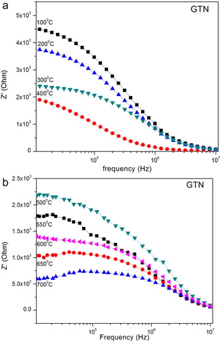
Fig. 12 (a–b) imaginary part of impedance with frequencies at 100–700 °C.
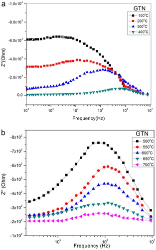
Fig. 13 Arrhenius plot for the sample GTN.
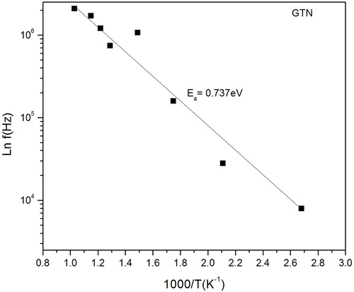
Arrhenius plot () shows that the peak frequency is a function of temperature. The activation energy is found to be 0.737 eV. The low value of activation energy is due to the higher mobility of oxygen vacancies. The ionization of oxygen vacancies create conduction electrons, which are thermally activated. Thus conductivity of the sample is increases as the temperature increases.
(a–b) shows the plot of Z′ and Z″ (Cole–Cole plot) at different temperatures. At low temperatures, we could observe only one peak, which represented the grain contribution, but there are two overlapping semi circles at high temperatures, one due to grain effect and other due to grain boundary effect [Citation34]. The grain boundary effect is due to its high resistance and high capacitance and it is visible only at low frequency side. The complex impedance or Nyquist plot indicates the presence of grain effect, which is found to decrease with increase in temperature. It suggests that the composition exhibits the NTCR behaviour usually shown by semiconductors. The semi conducting nature of the grains in ceramic is due to the loss of oxygen during high temperature sintering [Citation35].
Fig. 14 (a–b) Complex impedance spectrum of GTN at 100–700 °C.

5 Conclusion
RETiNbO6 (RE = Gd, Dy, Er, Yb) materials are prepared using modified combustion technique without the need of any calcination. XRD studies showed that all samples have orthorhombic euxenite structure with space group pbcn. FT-IR and Raman spectral analyses confirm that the as-prepared powders are phase-pure. The particle size obtained from Scherrer formula is in good agreement with TEM results. The dielectric properties are also studied in the low frequency range 50 Hz–2 MHz. The materials have good dielectric properties and hence they are suitable for communication systems. The high absorption intensities of the samples in UV region as well as high emission at visible range are very useful in screening off UV, optical amplifiers etc. The samples are good luminescent material with peaks at violet, blue and green regions.
The nano-crystalline samples are sintered around 1250 °C, which is much less than that of the conventional sample. SEM micrographs of the sintered samples show that samples have achieved maximum densification. Dielectric Impedance analysis indicates the presence of grain and grain boundary effect in the samples. The sample shows dielectric relaxation and the relaxation frequency shifted to higher frequency side with increase in temperature. It suggests that the composition exhibits the NTCR behaviour usually shown by semiconductors.
Acknowledgement
The authors acknowledge the Kerala State Council for Science, Technology and Environment, Government of Kerala for financial assistance.
References
- G.K.StrukovaV.V.KedrovV.N.ZverevS.S.KhasanovI.M.OvchinnikovI.E.BatovV.A.GasparovPhysica C2911997207212
- S.SolomonJ.T.JosephH.P.KumarJ.K.ThomasJ. Mater. Lett.60200628142818
- A.B.CorradiF.BondioliA.M.FerrariT.ManfrediniJ. Mater. Res. Bull.4120063844
- I.KomkovDokl. Akad. Nauk SSSR148196311821183
- H.SeifertB.BeckFortschr. Minerol.3919613639
- P.-S.ChangSci. Sin.12196323372343
- I.KomkovDokl. Akad. Nauk SSSR148196311821183
- V.B.AleksandrovDokl. Akad. Nauk SSSR1421963181184
- G.BlasseJ. Inorg. Nucl. Chem.28196611221124
- V.V.KazantsevE.I.KrylovA.K.BorisovA.I.ChupinJ. Inorg. Chem.191974506507
- C.E.HolcombeJ. Mater. Sci. Lett.14197922552260
- S.SolomonPhD thesis1999University of Kerala
- M.T.SebastianS.SolomonR.RatheeshJ. Am. Ceram. Soc.84200114871489
- A.K.TyagiS.V.ChavanR.D.PurohitIndian J. Pure Appl. Phys.442006113118
- A.K.TyagiR.D.PurohitIANCAS Bull.62007120131
- D.DhakP.DhakT.GhoraiS.K.BiswasP.PramanikJ. Mater. Sci. Mater. Electron.192008448456
- K.C.PatilS.T.ArunaT.MimaniCurr. Opin. Solid State Mater Sci.62002507517
- G.K.WilliamsonW.H.HallActa Metall.119532231
- S.J.ChiperaL.D.BishAdvances in X-ray Analysis341991PlenumNewYork325335
- W.G.FateleyF.R.DollishN.T.Mc DevittF.F.BentteyInfrared and Raman Selection Rules for Molecular and Lattice Vibrations: The Correlation Method1972John Wiley Inter scienceNew York
- N.G.ErorU.BalachandranJ. Solid State Chem.451982276279
- S.JosephM.K.SureshJ.K.ThomasA.JohnS.SolomonInt. J. Appl. Ceram. Technol.72010E129E134
- K.NakamotoInfrared and Raman Spectra of Inorganic and Coordination Compoundsfourth ed.1986John Wiley & SonsNew York
- K.C.MathaiS.VidyaSamSolomonJ.K.ThomasAdv. Mater. Res.22013277291
- J.C.MaxwellA Treatise on Electricity and Magnetism21954Oxford University PressOxford, UK328
- C.G.KoopsPhys. Rev.831951121
- X.QiT.P.J.HunH.G.GallangherB.HendersonR.IllingworthI.S.RuddockJ. Phys. Condens. Matter819964837
- LovelyJacobH.Padma KumarK.G.GopchandranJijimon K.ThomasSamSolomonJ Mater Sci: Mater. Electron.222011384388
- M.S.GudiksenJ.F.WangC.M.LieberJ. Phys. Chem. B10620024036
- S.VidyaAnnammaJohnSamSolomonJ.K.ThomasAdv. Mater. Res.132012191204
- R.PaylingP.LarkinsOptical Emission Lines of Elementsfirst ed.2000John Wiley and SonsNew York
- DhwajamJ.K.ThomasK.JoySamSolomonJ. Mater. Sci. Mater. Electron.201010.1007/s10854-010-0147-2
- B.BeheraP.NayakR.N.P.ChoudaryMater. Res. Bull.432008401
- H.RahmouniM.NouiriR.JemaiN.KallalF.RziguaA.SelmiK.KhirouniS.AlayaJ. Magn. Mater.316200723
- B.P.DasR.N.P.ChoudharyP.K.MahapatraIndian J. Eng. Mater. Sci.152008152156