
 ?Mathematical formulae have been encoded as MathML and are displayed in this HTML version using MathJax in order to improve their display. Uncheck the box to turn MathJax off. This feature requires Javascript. Click on a formula to zoom.
Abstract
The metal oxide semiconductor gas sensor technology is robust and has quick response times. In this work, aluminium and tin co-doped zinc oxide (ASZO) thin films were synthesized by a sol–gel dip-coating process as sensors for the greenhouse gas nitrogen dioxide (NO2). The prepared ASZO thin films were characterized using such techniques as X-ray diffraction (XRD), scanning electron microscopy (SEM), atomic force microscopy (AFM) and photoluminescence (PL) emission studies in order to analyze the elemental confirmation, particle size, surface roughness and optical emission properties, respectively. The XRD data reveals the hexagonal structure of ASZO and that the preferential orientation is along 2θ = 36.19°. SEM images of the ASZO thin film exhibit rod-like formations of ASZO on the substrate. The ASZO films show enhanced sensing behaviour, sensing NO2 gas even at 2 ppm at an operating temperature of 170 °C. The response and recovery times were determined to be 30 and 20 s, respectively.
1 Introduction
Trace gases play an important role in atmospheric composition, radiative interaction, climate change and pollution, despite their small concentrations. Increase in the atmospheric percentage of these trace gases due to human activities, such as the burning of fossil fuels [Citation1,Citation2], causes major issues, including respiratory diseases, ozone depletion, global warming, and acid rain. Therefore, it is essential to monitor and mitigate toxic air pollutants, resulting in the need for gas sensors. NO2 is a very important trace gas because it is one of the precursors which are highly poisonous, reactive and potentially harmful to ozone [Citation3–Citation9]. Seven oxides of nitrogen are found in ambient air. These include NO, NO2, NO3, N2O, N2O3, N2O4 and N2O5. NO and NO2 and are collectively known as NOx because they are rapidly interconverted during the day. NOx pollution is caused due to excessive emission from automobiles, trucks, industrial sources and various non-road vehicles (e.g., construction equipment and boats). Because NOx is an oxidizing agent, it reacts with volatile organic compounds (VOC) in the atmosphere to form complex compounds. NOx affects the mucosa of the eyes, nose, throat and respiratory tract, and also causes irritation. Continuous exposure to NOx gas leads to various respiratory conditions, such as decreased lung function, pulmonary diseases, acute or chronic bronchitis, pulmonary oedema, and diffuse lung injury [Citation10–Citation14]. Thus, it is very essential to monitor and mitigate this pollutant. Currently, sensors for monitoring trace gases are imported from other countries and are highly costly. As per current literature, ZnO thin film-based gas sensors show promising results as sensors for atmospheric gases [Citation5,Citation15–Citation19].
Zinc oxide is an inorganic semiconductor compound with the formula ZnO. In materials science, ZnO is classified as a wide bandgap semiconductor from the II–VI group. ZnO thin films can act as effective sensors due to their various properties such as high electron mobility, transparent conducting behaviour, etc. [Citation20–Citation25]. The electrical characteristics of semiconducting metal oxide materials change when there is a variation in the composition of the surrounding gas. The development of gas sensors based on this effect, using thin films of n-type zinc oxide is in progress. However, this type of gas sensor shows a lack of selectivity due to a non-specific gas detection mechanism, resulting in the detection of many types of reducing gases. Therefore, to fabricate selective sensors, different impurities such as Sn, Fe, Cu, Al, etc. are added as dopants to the ZnO thin films. ZnO thin films have been extensively studied by many researchers for applications in efficient gas sensing. To meet with demands for several applications, such impurities as F, B, Al, Ga, In, and Sn are added to the ZnO nanoparticles in order to increase their conductivity. ZnO nanorod-based H2 and O3 sensors have been prepared by molecular beam epitaxy and exhibit sensitivity towards ozone (O3) at room temperature and towards H2 at 112 °C [Citation26]. When the ZnO nanorods are sputter-coated with Pd or Pt, the sensitivity is increased by a factor of 5, and these sensors can detect H2 down to concentrations of 10 ppm at 25 °C [Citation27]. The transparent, conductive nature of the ZnO thin films, essential for gas sensor fabrication, is greatly enhanced by doping it with Al [Citation28]. Therefore, carrier mobility and concentration can be drastically increased by the addition of Al as a dopant [Citation29]. Additionally, Sn-doped ZnO thin films show enhanced sensitivity to NO2 gas, and the sensitivity is better than that of undoped ZnO [Citation5]. The literature indicated that there was only limited research on the topic of Al and Sn co-doped ZnO thin films as gas sensors. Therefore, this work shows the preparation of Al and Sn co-doped ZnO thin films as NO2 gas sensors and also investigates their sensing properties.
2 Experimental
2.1 Preparation of ASZO
ASZO thin films were prepared using a conventional dip-coating method. The sol was prepared using zinc acetate dihydrate, diethanolamine (DEA), and isopropanol as precursors. Equimolar quantities of zinc acetate (1 M) and DEA (1 M) were maintained in the precursor solution. Tin was added as a dopant by introducing 4 ml of SnCl2·2H2O dissolved in ethanol (0.2 M) into the above mixture. The solution was then heat-refluxed for 1 h at 70 °C. To dope with aluminium, a solution containing 0.2 M aluminium nitrate dissolved in ethanol was added to the previous mixture. A clear and homogeneous solution was obtained by stirring at 70 °C for 2 h. The prepared ASZO solution was then aged for 24 h to make it suitable for coating.
2.2 Preparation of thin films
The glass slide to be coated was sonicated in acetone for 20 min to obtain a dust-free substrate. The dip-coating process was carried out for with an average dip time of 30 min, and dry time was maintained at 60 and 30 s, respectively. The prepared sample was kept in a hot-air oven at 100 °C for an hour followed by calcination of the thin film at 500 °C for 1 h to ensure crystallization and to remove unreacted precursors and impurities.
3 Results and discussion
3.1 X-ray diffraction
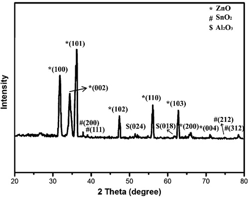
The diffraction pattern of the thin film calcinated at 500 °C exhibited eight Bragg peaks, among which the peak at 2θ = 36.19° was prominent, as shown in . Therefore, the preferential orientation was along (101) with the d-spacing of 0.248 nm. The 2θ values of all the samples were well-matched with JCPDS No. 89-1397 [Citation30]. Because the doping concentrations of Al and Sn were very low in comparison to ZnO, the diffraction peaks for Al and Sn were much reduced in the XRD pattern which showed dominant ZnO peaks. The XRD peaks for SnO2 and Al2O3 were in good agreement with JCPDS Nos. 88-0287 and 81-1667, respectively. The prepared ASZO thin films showed monophasic and polycrystalline hexagonal structure.
Fig. 1 X-ray diffraction pattern of ASZO film.
The crystallite size of the ASZO formed on the glass substrate can be calculated using the formula,(1)
(1) where λ is the wavelength of the X-ray (0.15406 nm), β is full-width half maximum (FWHM) of the corresponding diffraction peak (hkl) and θ is the Bragg diffraction angle. The crystallite size calculated from the XRD data was larger in value. This is because of the high calcination temperature, at which the crystallites merge with each other resulting in larger crystallites. The strain associated with the ASZO thin film can be calculated using the expression below,
(2)
(2)
From , the calculated strain value was very low due to the release in strain associated with ASZO, during annealing. The number of dislocations in a unit volume of crystalline material can be determined by the dislocation density. The dislocation density, which can be defined as the number of defects in the film was determined by the formula,(3)
(3)
Table 1 Structural parameters of ASZO thin film.
The calculated structural parameters are tabulated in .
3.2 SEM analysis
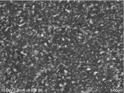
shows the SEM image of the prepared ASZO thin film. The SEM micrograph was taken with a magnification of 8000× at an operating voltage of 10 kV. The ASZO particles, which could be visualized from the SEM micrograph, were distributed evenly over the substrate. The particle size of ASZO particles on the glass substrate varied from 100 to 200 nm.
Fig. 2 SEM micrograph of ASZO thin film.
3.3 AFM studies
shows the topographical image of ASZO thin film, as obtained by AFM. From the figure, the average particle size distribution in the ASZO film was found to be approximately 200 nm. Surface roughness, skewness and kurtosis of the ASZO thin film were calculated using the obtained AFM data and are tabulated in . The thickness of the film, RMS roughness (Rq), and average roughness (Ra) of the thin film was interpreted and their values are 227.739 nm, 66.215 nm, and 50.229 nm, respectively. Roughness skewness (Rsk) is used to study the symmetrical behaviour of surface variations about a mean line. Rsk is more sensitive to deep valleys and high peaks. The negative skewness obtained for the ASZO thin film was due to the presence of more valleys than peaks. Roughness kurtosis (Rku) is the expression to determine the distribution of spikes about a mean line. For spiky surfaces, Rku is greater than 3; for rough surfaces, Rku is less than 3; and for random surfaces, Rku is 3. The Rku obtained for the ASZO thin film shows a value greater than 3, indicating the surface is spiky which can be well understood from the AFM image.
Fig. 3 AFM studies of ASZO thin film.
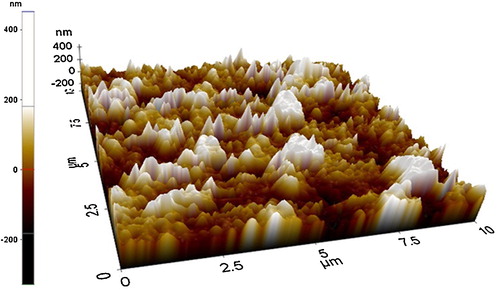
Table 2 Results obtained from AFM studies.
3.4 Photoluminescence (PL) spectra
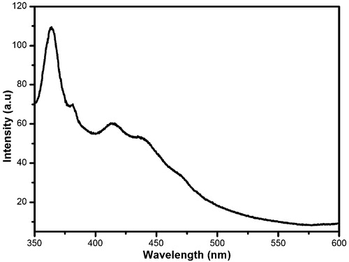
The PL spectrum of the prepared thin films was analyzed with an excitation wavelength of 325 nm, in the range from 350 to 600 nm. From , it is seen that the ASZO thin film showed four peaks; a major peak at 364 nm and three minor peaks at 381, 412 and 431 nm, respectively. The UV band showed two peaks at 364 nm and 381 nm which were attributed to near-band edge emission [Citation31]. The emission at 364 nm was due to the electron transition from excitons bound to donors, and the emission at 381 nm was attributed to donor-acceptor pair recombination. The two low-intensity peaks found in the violet-blue region at 412 and 431 nm, respectively, were attributed to deep-level emissions. The reason for the blue emissions is not known conclusively and debates are ongoing, considering various aspects such as oxygen vacancy (VO), zinc vacancy (VZn), oxygen interstitial (Oi), zinc interstitial (Zni), oxygen anti-site (OZn) and zinc anti-site (ZnO) [Citation32]. All of these phenomena contribute to the deep-level emissions.
Fig. 4 PL emission spectra of ASZO film.
3.5 Gas sensing analysis
In order to characterize sensor performance, a set of parameters was used, including sensitivity, recovery and response times, and working temperature [Citation33]. The gas-sensing mechanism in oxide-based devices is governed by the reactions with gas molecules, occurring at the surface of the metal oxide. The mechanism initiates with the chemisorption of oxygen molecules over the surface of the ASZO thin film, followed by the charge transfer phenomenon between the test gas and the adsorbed oxygen molecules [Citation34]. When there is a charge transfer phenomenon, the resistance of the thin film changes. The presence of oxidizing gases increases the film resistance while the presence of reducing gases reduces the resistance. In order to measure the sensor resistance in a desired concentration of the analyte gas, a known concentration of gas in ppm was injected into the housing using a micro–syringe. The volume of the test chamber was 10 l. Therefore, to measure the response of the sensor for 1 ppm, 10 μl of the test gas was injected into the test chamber. The resistance of the sensor as a function of time was measured. The recovery of the sensor was studied by analysing the variation in resistance after removing the sensor and exposing it to air. The sensor responses for oxidizing and reducing gases can be calculated using the following expressions:(4)
(4)
(5)
(5) where Rg and Ra are the resistance of the sensing element influenced by gas concentration and by air, respectively, and C is the gas concentration in ppm. The operating temperature is one of the most important properties of the as-prepared gas sensor. The optimal operating temperature is closely related not only to the properties of the material itself but also to the gas-sensing process of the gas towards the surface of materials. For the prepared ASZO thin films, the operating temperature was determined to be 170 °C and is represented in (a).
Fig. 5 (a) Temperature dependent sensitivity of the ASZO thin film. (b) Response behaviour of ASZO thin film. (c) Sensitivity of Sensor against gas concentration.
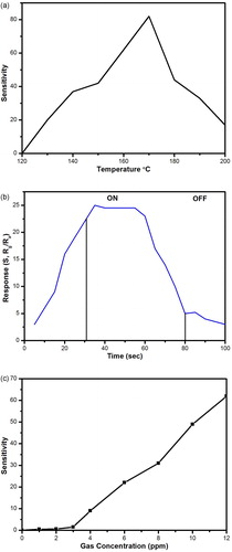
It is evident from the figure that the sensitivity increased with increased temperature, reached a maximum at 170 °C, and gradually declined thereafter. This finding is observed due to the loss of adsorbed oxygen on the surface of the thin film with the increase in temperature. This results in further increase in electron concentration on the thin film surface, improves the film conductivity, and thus increases the sensitivity. This phenomenon results in decreased electron conduction at low temperatures and enhanced conduction at higher temperatures. Response time and the recovery time are the other major parameters to be considered. Response time is defined as the time required to reach 90% of the saturation response and the recovery time can be calculated as the time taken by the sensor to recover 90% of the response when the gas flow is switched off and subsequently filled with air. The response time and recovery time of the sensor were approximately 30 and 20 s, respectively, as shown in (b). Desorption is an irreversible process whereby the resistance is stabilized for few seconds, which results in a delay in recovery time. (c) shows the increase in sensitivity of the prepared thin film with increasing test gas concentration. From the figure, it is seen that the sensitivity drastically increased with increasing concentration of the test gas and the sensing behaviour started at NO2 gas concentrations of 2 ppm. The fabricated sensor showed good sensitivity and a fast response time (30 s) to the NO2 gas. Additionally, the operating temperature and the power consumptions were greatly decreased compared to previous reports of un-doped ZnO [Citation35] and Ga-doped ZnO film [Citation36].
4 Conclusions
The Al-Sn co-doped ZnO thin film sensor was fabricated using a sol–gel process. ASZO thin films were characterized using XRD, SEM, AFM, and PL emission spectra. Sensing characteristics of the ASZO thin film sensor were also studied. The ASZO thin films showed an average thickness of 227 nm (derived from AFM data) and exhibited good sensitivity towards NO2. The ASZO thin film sensors showed better performance, sensing NO2 gas even at 2 ppm under an operating temperature of 170 °C. The response time and recovery time were measured to be 30 and 20 s, respectively.
Acknowledgements
We thank the management and the principal of Mepco Schlenk Engineering College for providing facilities and constant encouragement for the successful completion of the project.
Notes
Peer review under responsibility of Taibah University.
Related Research Data
References
- S.HameedJ.DignonGlobal emissions of nitrogen and sulfur oxides in fossil fuel combustion 1970–1986J. Air Waste Manag. Assoc.422015159163
- A.RichterJ.P.BurrowsH.NüßC.GranierU.NiemeierIncrease in tropospheric nitrogen dioxide over China observed from spaceNature4372005129132
- M.A.Gomez-GarcıaV.PitchonA.KiennemannPollution by nitrogen oxides: an approach to NOx abatement by using sorbing catalytic materialsEnviron. Int.312005445467
- J.B.MilfordA.G.RussellG.J.McRaeA new approach to photochemical pollution control: implications of spatial patterns in pollutant responses to reductions in nitrogen oxides and reactive organic gas emissionsEnviron. Sci. Technol.23198912901301
- S.T.ShishiyanuT.S.ShishiyanuO.I.LupanSensing characteristics of tin-doped ZnO thin films as NO2 gas sensorSens. Actuators B: Chem.1072005379386
- M.ChenZ.WangD.HanF.GuG.GuoPorous ZnO polygonal nanoflakes: synthesis, use in high-sensitivity NO2 gas sensor, and proposed mechanism of gas sensingJ. Phys. Chem. C11520111276312773
- S.PengK.ChoP.QiH.DaiAb initio study of CNT NO2 gas sensorChem. Phys. Lett.3872004271276
- S.T.ShishiyanuT.S.ShishiyanuO.I.LupanNovel NO2 gas sensor based on cuprous oxide thin filmsSens. Actuators B: Chem.1132006468476
- A.GoldW.A.BurgessE.V.CloughertyExposure of firefighters to toxic air contaminantsAm. Ind. Hyg. Assoc. J.391978534539
- M.G.MustafaD.F.TierneyBiochemical and metabolic changes in the lung with oxygen, ozone, and nitrogen dioxide toxicityAm. Rev. Respir. Dis.118197810611090
- M.A.LovichN.K.BrunoC.P.PlantA.E.WeiG.B.VasquezB.J.JohnsonD.H.FineR.J.GilbertUse of ultra-pure nitric oxide generated by the reduction of nitrogen dioxide to reverse pulmonary hypertension in hypoxemic swineNitric Oxide242011204212
- P.J.BarthS.UhlarikA.BittingerU.WagnerJ.RuschoffDiffuse alveolar damage in the rat lung after short and long term exposure to nitrogen dioxidePathol. Res. Pract.19019943341
- I.Y.HaddadG.PatakiP.HuC.GallianiJ.S.BeckmanS.MatalonQuantitation of nitrotyrosine levels in lung sections of patients and animals with acute lung injuryJ. Clin. Investig.94199424072413
- E.D.AmsterM.HaimJ.DubnovD.M.BrodayContribution of nitrogen oxide and sulfur dioxide exposure from power plant emissions on respiratory symptom and disease prevalenceEnviron. Pollut.18620142028
- V.GalstyanE.CominiC.BarattoG.FagliaG.SberveglieriNanostructured ZnO chemical gas sensorsCeram. Int.4120151423914244
- T.-Y.ChenH.-I.ChenC.-S.HsuC.-C.HuangJ.-S.WuP.-C.ChouW.-C.LiuCharacteristics of ZnO nanorods-based ammonia gas sensors with a cross-linked configurationSens. Actuators B: Chem.2212015491498
- S.ÖztürkA.KösemenZ.A.KösemenN.KılınçZ.Z.ÖztürkM.PenzaElectrochemically growth of Pd doped ZnO nanorods on QCM for room temperature VOC sensorsSens. Actuators B: Chem.2222016280289
- R.ZhouG.HuR.YuC.PanZ.L.WangPiezotronic effect enhanced detection of flammable/toxic gases by ZnO micro/nanowire sensorsNano Energy122015588596
- S.P.UshaS.K.MishraB.D.GuptaFiber optic hydrogen sulfide gas sensors utilizing ZnO thin film/ZnO nanoparticles: a comparison of surface plasmon resonance and lossy mode resonanceSens. Actuators B: Chem.2182015196204
- M.CaglarS.RuzgarInfluence of the deposition temperature on the physical properties of high electron mobility ZnO films by sol–gel processJ. Alloys Compd.6442015101105
- R.S.AjimshaA.K.DasP.MisraM.P.JoshiL.M.KukrejaR.KumarT.K.SharmaS.M.OakObservation of low resistivity and high mobility in Ga doped ZnO thin films grown by buffer assisted pulsed laser depositionJ. Alloys Compd.63820155558
- W.M.KimJ.S.KimJ.-h.JeongJ.-K.ParkY.-J.BaikT.-Y.SeongAnalysis of optical band-gap shift in impurity doped ZnO thin films by using nonparabolic conduction band parametersThin Solid Films5312013430435
- C.-s.TianX.-l.ChenJ.-m.LiuD.-k.ZhangC.-c.WeiY.ZhaoX.-d.ZhangWide-spectrum Mg and Ga co-doped ZnO–TCO thin films with introduced hydrogen grown by magnetron sputtering at room temperatureAppl. Surf. Sci.3142014786793
- M.SouissiA.FouzriG.SchmerberHighlighting of ferromagnetism above room temperature in Cd-doped ZnO thin films grown by MOCVDSolid State Commun.21820154044
- G.ShanmuganathanI.B.Shameem BanuRoom temperature optical and magnetic properties of (Cu, K) doped ZnO based diluted magnetic semiconductor thin films grown by chemical bath deposition methodSuperlattices Microstruct.752014879889
- B.S.KangY.W.HeoL.C.TienD.P.NortonF.RenB.P.GilaS.J.PeartonHydrogen and ozone gas sensing using multiple ZnO nanorodsAppl. Phys. A: Mater. Sci. Process.80200510291032
- H.T.WangB.S.KangF.RenL.C.TienP.W.SadikD.P.NortonS.J.PeartonM.J.LinHydrogen-selective sensing at room temperature with ZnO nanorodsAppl. Phys. Lett.86200513
- L.WenM.KumarB.B.SahuS.B.JinC.SawangratK.LeksakulJ.G.HanAdvantage of dual-confined plasmas over conventional and facing-target plasmas for improving transparent-conductive properties in Al doped ZnO thin filmsSurf. Coat. Technol.28420158589
- ManishKumarLongWenBibhuti B.SahuJeon GeonHanSimultaneous enhancement of carrier mobility and concentration via tailoring of Al-chemical states in Al-ZnO thin filmsAppl. Phys. Lett.1062015241903
- K.JeyasubramanianaG.S.HikkuR.Krishna SharmaPhoto-catalytic degradation of methyl violet dye using zinc oxide nano particles prepared by a novel precipitation method and its anti-bacterial activitiesJ. Water Process Eng.820153544
- O.SenthilkumarK.YamauchiK.SenthilkumarT.YamamaeY.FujitaN.NishimotoUV-blue light emission from ZnO nanoparticlesJ. Korean Phys. Soc.5320084649
- M.WillanderO.NurS.ZamanA.ZainelabdinN.BanoI.HussainZinc oxide nanorods/polymer hybrid heterojunctions for white light emitting diodesJ. Phys. D: Appl. Phys.44201116
- B.PerretP.GrundlerChemical sensors. An introduction for scientists and engineersAnal. Bioanal. Chem.39220082122
- P.EsserW.GöpelPhysical adsorption on single crystal zinc oxideSurf. Sci.971980309318
- N.KoshizakiT.OyamaSensing characteristics of ZnO-based NOx sensorSens. Actuators B: Chem.662000119121
- H.-S.HwangJ.-T.SongD.-H.YeoH.-S.ShinY.-W.HongJ.-H.KimD.G.LimCharacteristics of a NOx sensor based on a low temperature Co-fired ceramic and Ga-doped ZnOJ. Korean Phys. Soc.53200813841387